15-1 / N. Chopra
• IMID 2009 DIGEST
Abstract
In this paper, we study effect of charge balance on performance of blue phosphorescent organic light emitting diodes (OLEDs). Charge balance determines the location of recombination zone in the OLEDs. By tuning the charge balance in iridium (III) bis[(4,6-di-fluorophenyl)-pyridinate-N,C2`]picolinate (FIrpic) based blue phosphorescent organic light-emitting devices (PHOLEDs) with a high mobility and high triplet energy electron transporting material, we were able to achieve a high current efficiency of 60 cd/A which is a 3X improvement over previous devices with 3,5´-N,N´-dicarbazole-benzene (mCP) host.
1. Introduction
Organic light emitting diodes (OLEDs) have recently received much of attention due to their potential applications in solid state lighting and flat-panel displays[1]. Since the seminal work by Tang
and Van Slyke[2], a lot of progress has been made in
the field of OLEDs. OLEDs offer numerous advantages for display and lighting applications over their conventional counterparts[3] such as low power
consumption, wide viewing angle, fast response time, compact and light-weight[4]. The development of
phosphorescent OLEDs[5] made it possible to achieve
very high quantum efficiencies in these devices[6].
Efficiency for blue PHOLEDs is generally lower as compared to their green counterparts[6] because wide
band gap materials with high triplet energies are required for efficient carrier confinement on dopant molecules which are difficult to design and synthesize. These wide band gap materials generally have poor charge injection and transporting behavior.
For maximizing the efficiency of blue PHOLEDs
the two most important factors are: 1) Using High triplet energy materials to reduce triplet quenching[7]
and 2) charge balance in the device[8]. Charge
balance is a very important factor in the performance of an OLED. Imbalance in charge transport can lead to accumulation of charges in an OLED heterostructure thereby leading to loss in efficiency[9]
and lifetime[10]. However, carrier transport in most
OLED devices is highly imbalanced[11]. For
example, the hole mobility in commonly used organic hole transport materials (HTMs) such as 4,4′
-bis[N-(1-naphthyl)-N-phenyl-amino]biphenyl (NPD) or 1,1-bis[(di-4-tolylamino) phenyl] cyclohexane (TAPC)[12] is about three orders of magnitude higher
than the electron mobility of electron transport materials such as tris(8-quinolinolato)aluminum (Alq3) or 2,9-dimethyl-4,7-diphenyl-1,10-phenanthroline (BCP)[13]. Hence, charge imbalance
can cause the recombination zone to move from the bulk of emitting layer to the interface. This makes the charge balance a much more important factor in case of PHOLEDs. In addition, triplet energies of commonly used hole and electron transport materials such as NPD (triplet energy, T1=2.29 eV), BCP (T1=2.5 eV) and Alq3 (T1= 2.0 eV) are lower than that of commonly used blue phosphorescent dopant Iridium(III) bis [(4,6-di-fluorophenyl)- pyridinato-N,C2´] picolinate (FIrpic, T1=2.7 eV)[12]. Hence, if the recombination zone is at the interface then the excitons can be quenched by lower triplet energy charge transporting layer. Therefore, charge balance plays an important role in achieving high efficiency PHOLEDs.
In this letter, we investigate the charge balance in FIrpic-based OLEDs by studying the charge transport properties of the corresponding electron-only and
Charge Balance in High Efficiency Blue Phosphorescent
Organic Light Emitting Diodes
Neetu Chopra, Jaewon Lee and Franky So
Departement of Materials Science and Engineering, University of Florida, Gainesville, FL 32611, USA
Tel.:+1-352-846-3790, E-mail: [email protected]
15-1 / N. Chopra
IMID 2009 DIGEST •
hole-only devices. The device data indicate that the carrier transport is strongly hole dominant and the recombination zone is located at the electron transport layer (ETL) interface. Using a high mobility, high triplet energy ETL, we were able to achieve better charge balance and a maximum current efficiency of 60 cd/A at a luminance of 500 cd/m2 was achieved
2. Experimental
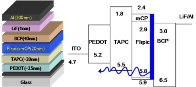
The OLEDs and the single carrier device were fabricated on pre-patterned ITO substrates with a sheet resistance of 20 Ω per square. Substrates were cleaned via sonication in detergent, de-ionized (DI) water, acetone, isopropyl alcohol, DI water followed by UV ozone treatment. Devices were fabricated by spin coating the PEDOT: PSS (~25 nm) layer on ITO glass substrate. The film was then baked at 180°C to evaporate the solvent. This layers serves to facilitate better hole injection. All other layers were vacuum deposited at a pressure of 2X10⁻⁶ Torr. TAPC (20 nm) was used a hole transporting material and mCP (20 nm) doped with 2-3% of FIrpic is used the emitting layer (EML). BCP (40 nm) is used as hole blocker/ electron transporting layer (ETL). The cathode consisted of a 1 nm thick layer of LiF followed by a 100 nm thick Al. Figure 1 shows the device structure for control OLED device and corresponding energy diagram.
Fig. 1. Device structure and energy level diagram.
3. Results and discussion
As discussed above, usually the hole mobility of HTL is much higher than electron mobility of ETL which leads to charge imbalance in small molecule based organic devices. In our device structure also, there is a significant imbalance in charge transport. The hole mobility of TAPC (~ 1.0X10⁻² cm2/Vs)[12] is four orders of magnitude higher than the electron
mobility of BCP (5.5X10⁻⁶ cm2/Vs)[13]. Hence, it is expected that the OLED device is strongly hole dominant and the recombination zone is near the ETL (BCP) interface. Since the triplet energy of BCP is lower than that of FIrpic, triplet exciton quenching is expected at the BCP interface. To study the charge imbalance in this OLED structure, single carrier devices corresponding to the OLED were also fabricated. The hole-only device has the following structure: ITO/ PEDOT:PSS (25 nm)/ HTL (200 nm)/ EML (20 nm)/Au, and the electron-only device has the following structure: ITO/EML (20 nm)/ ETL (200 nm)/ LiF (1 nm) /Al. Current-voltage measurements were performed on these devices. From the current density-voltage (J-V) data shown in Fig. 2 it can be seen clearly that the hole current density is more than four orders of magnitude higher than the electron current density over a wide voltage range.
0 2 4 6 8 10 10-6 10-5 10-4 10-3 10-2 10-1 100 101 102
Electron only device Hole only device
Cu rre nt De ns ity [ mA /cm 2] Voltage [V]
Fig. 2. J-V characteristics for single-carrier devices.
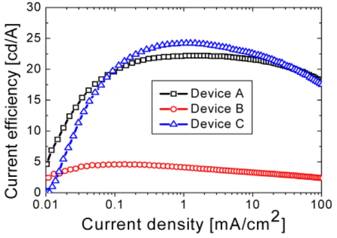
Three different OLEDs were fabricated to probe the location of recombination zone and charge balance in the device. Device A is the control device with the entire emitting layer doped with FIrpic with the following structure: ITO/PEDOT/TAPC/mCP: FIrpic (20 nm) /BCP /LiF/Al; device B (left-doped) has a partially FIrpic-doped emitting layer adjacent to the HTL with the following structure: ITO/PEDOT/TAPC/mCP: FIrpic (10 nm) /mCP (10 nm)/BCP/LiF/Al; device C (right-doped) has a partially FIrpic-doped host layer adjacent to the ETL with the following structure: ITO/PEDOT/TAPC/mCP (10 nm)/mCP: FIrpic (10 nm) /BCP/LiF/Al. Since the device is electron deficient, only a small fraction of electrons will be able to transport across the undoped host layer, and device B should have lower efficiency. If the recombination is indeed located at the ETL
15-1 / N. Chopra • IMID 2009 DIGEST 0.010 0.1 1 10 100 5 10 15 20 25 30 C ur re nt e ffi ci en cy [c d/ A ]
Current density [mA/cm2]
Device A Device B Device C
interface, the efficiency of device C should be similar to that of the control device A. It should be noted that in devices with mCP as a host, the charge carriers are transported through mCP and the presence of FIrpic does not affect the carrier transport in the emitting layer[14]. Therefore, the exact location of the doped
layer should not affect the carrier transport in the mCP layer. The LIV characteristics of these devices are shown in Figure 3a). The data show that there is no significant difference in the IV characteristics among the three devices, and these results are expected since FIrpic does not affect carrier transport in the host layer. However, device B has a substantially lower luminance compared to devices A and C indicating that it has lower efficiency. The efficiencies of these three devices are also shown in Figure 3b). The current efficiency of device B is less than 5 cd/A which is substantially lower compared to the other two devices (> 20 cd/A). The results indicate that in device B only a small portion of the electrons injected are able to transport across the undoped host layer and recombine with holes injected from the HTL resulting in low efficiency. Based on the data, it is apparent that in both devices A and C the recombination zone is located at the BCP interface. However, since BCP has lower triplet energy than FIrpic, recombination at the BCP interface leads to triplet exciton quenching. If BCP is replaced with electron transport materials with higher electron mobility and higher triplet energy, charge balance will be improved and exciton quenching will be reduced resulting in higher overall device efficiency.
Fig. 3. Current efficiency for devices A, B and C.
In our present study, to show the effect of charge balance on device performance we chose two other ETLs to compare with BCP. The two materials used for comparison are: tris[3-(3-pyridyl)-mesityl]borane
(3TPYMB) and 4,7-diphenyl-1,10-phenanthroline (BPhen). We chose 3TPYMB since its electron mobility (~10-5 cm2V-1s-1)[15] is about an order of magnitude higher than that of BCP and it has one of the highest triplet energy (T1=2.98 eV) amongst all electron transport materials (ETMs) used in OLEDs. BPhen (T1=2.5 eV) was also chosen since it has triplet energy similar to that of BCP while its electron mobility (10-4 cm2V-1s-1) is the highest amongst all three ETMs.
To demonstrate the effect of charge balance on OLED device performance we fabricated devices with the three different electron transport materials. Figure 4 shows the device efficiencies for all three devices. The BCP device has the lowest efficiency of all which is in agreement with its lowest mobility and low triplet energy. Although the electron mobility of BPhen is substantially higher than those of the other two ETMs, due to its low triplet energy, the device efficiency is only slightly higher than that of the BCP device. Finally, the 3TPYMB device shows substantially higher efficiency (60 cd/A) compared to the other two devices. Similar efficiency has also been reported for FIrpic based devices. Also because of the better charge balance in the device, the device shows quite good roll-off characteristics and has high efficiency of 57 cd/A even at 1000 cd/m2. The results demonstrate that both high mobility and high triplet energy electron transport materials are required for high device efficiency.
100 101 102 103 104 0 10 20 30 40 50 60 70 3TPYMB BCP Bphen C ur re nt e ffi ci en cy [C d/ A ] Luminance [Cd/m2]
Fig. 4. Current efficiencies for OLED devices with BCP, 3TPYMB and BPhen as the ETL.
4. Conclusion
In summary, charge balance was studied in FIrpic-based blue phosphorescent OLEDs by fabricating single carrier devices and the devices were found to
15-1 / N. Chopra
IMID 2009 DIGEST •
be hole dominant. We found that the recombination zone is located at the EML/ETL interface by selectively doping FIrpic in different regions of the host. Using 3TPYMB, the charge balance is enhanced. Because of the high electron mobility and high triplet energy in the electron transport layer, a maximum efficiency of 60 cd/A (50 lm/W) was demonstrated.
5. References
1. B. C. Krummacher, V.-E. Choong, M. K. Mathai,
S. A. Choulis, F. So, F. Jermann, T. Fiedler, M. Zachau,
Applied Physics Letters2006, 88, 113506.
2. C. W. Tang, S. A. VanSlyke, Applied Physics
Letters1987, 51, 913.
3. A. R. Duggal, J. J. Shiang, M. H. Christian, F. F.
Donald, Applied Physics Letters2002, 80, 3470.
4. S. R. Forrest, Nature2004, 428, 911.
5. M. A. Baldo, D. F. O'Brien, Y. You, A.
Shoustikov, S. Sibley, M. E. Thompson, S. R. Forrest,
Nature1998, 395, 151.
6. M. A. Baldo, S. Lamansky, P. E. Burrows, M. E.
Thompson, S. R. Forrest, Applied Physics Letters1999, 75,
4.
7. K. Goushi, R. Kwong, J. J. Brown, H. Sasabe, C.
Adachi, Journal of Applied Physics2004, 95, 7798.
8. C. Adachi, M. A. Baldo, M. E. Thompson, S. R.
Forrest, Journal of Applied Physics2001, 90, 5048.
9. J.-H. Lee, T.-C. Lin, C.-C. Liao, F. H. Yang,
"Study on organic light-emitting device with more balanced
charge transport", presented at SPIE, 2005.
10. V.-E. Choong, S. Shi, J. Curless, C.-L. Shieh, H.
C. Lee, F. So, J. Shen, J. Yang, Applied Physics Letters
1999, 75, 172.
11. F. So, B. Krummacher, M. K. Mathai, D.
Poplavskyy, S. A. Choulis, V.-E. Choong, Journal of
Applied Physics2007, 102, 091101.
12. J. Lee, N. Chopra, S.-H. Eom, Y. Zheng, J. Xue,
F. So, J. Shi, Applied Physics Letters2008, 93, 123306.
13. Y. Q. Li, M. K. Fung, Z. Xie, S. T. Lee, L. S.
Hung, J. Shi, Advanced Materials2002, 14, 1317.
14. R. J. Holmes, S. R. Forrest, Y. J. Tung, R. C.
Kwong, J. J. Brown, S. Garon, M. E. Thompson, Applied
Physics Letters2003, 82, 2422.
15. D. Tanaka, T. Takeda, T. Chiba, S. Watanabe, J.