IntroductIon
As the modern industrial products continue to become more sophisticated in their structure, the importance of X-ray non-destructive test(NDT) has also been increas-ing recently. For light and small electronic objects such as cellular phones, a low-energy X-ray inspection using the energy range from 20 to 150 keV has been widely used
to-gether with amorphous flat panel detectors or CMOS image sensors for 2-D and 3-D imaging(Zentai 2011). However, for heavy and large objects such as cargo containers, only a linear scan system has been used because of their large geometry(Butt 2014; Xiao et al. 2016). Recently the X-ray application extends to the in-line quality inspection for au-tomobiles, aircrafts, rockets, missiles and spacecraft launch-ers. Also the 3-D computed tomography has been more widely adopted because it can provide cleaner image by removing the overlapping nature of 2-D radiography(Martz
Design of a Linear Detector Array Unit for High Energy X-ray
Helical Computed Tomography and Linear Scanner
Jeong Tae Lee1, Jonghwan Park1,2, Hyunduk Kim2, Giyoon Kim1, Dong Geun Kim3,Shin-Woong Park4, Yun Yi4 and Gyuseong Cho1,*
1Department of Nuclear and Quantum Engineering, Korea Advanced Institute of Science and Technology(KAIST), Daejeon 34141, Republic of Korea 2Research Center, Luvantix ADM Co., Ltd., Daejeon 34051, Republic of Korea 3Medical Imaging Department, ASTEL Inc., Seongnam Gyeonggi-do 13486, Republic of Korea 4Department of Electronics and Information Eng, Korea University, Seoul 02841, Republic of Korea
Abstract - A linear detector array unit(LdAu) was proposed and designed for the high energy
X-ray 2-d and 3-d imaging systems for industrial non-destructive test. Specially for 3-d imaging,
a helical ct with a 15MeV linear accelerator and a curved detector is proposed. the arc-shape
detector can be formed by many LdAus all of which are arranged to face the focal spot when the source-to-detector distance is fixed depending on the application. An LdAu is composed of 10
modules and each module has 48 channels of cdWo4(cWo) blocks and Si PIn photodiodes with
0.4mm pitch. this modular design was made for easy manufacturing and maintenance. through
the Monte carlo simulation, the cWo detector thickness of 17mm was optimally determined.
the silicon PIn photodiodes were designed as 48 channel arrays and fabricated with ntd(neutron
transmutation doping) wafers of high resistivity and showed excellent leakage current properties
below 1nA at 10V reverse bias. to minimize the low-voltage breakdown, the edges of the active
layer and the guard ring were designed as a curved shape. the data acquisition system was also designed and fabricated as three independent functional boards; a sensor board, a capture board
and a communication board to a Pc. this paper describes the design of the detectors(cWo
blocks and Si PIn photodiodes) and the 3-board data acquisition system with their simulation results.
Key words : High energy X-ray, Helical ct, non-destructive test(ndt), Linear accelerator (LInAc),
Linear detector array unit(LdAu), cWo, Si PIn photodiode, data acquisition system
(dAS)
─ 145 ─ Technical Paper
Journal of Radiation Industry 10(3) : 145~152(2016)
* Corresponding author: Gyuseong Cho, Tel. +82-42-350-3821, Fax. +82-42-350-5861, E-mail. [email protected]
et al. 1990).
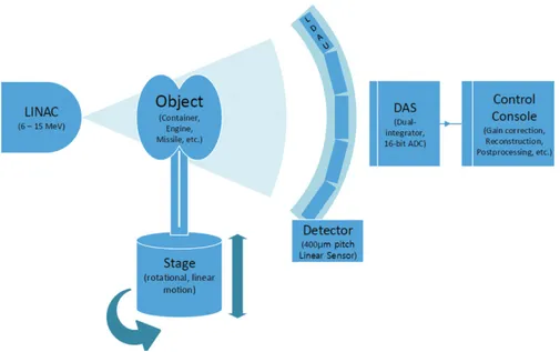
We are currently developing a linear accelerator(LINAC) based high energy X-ray imaging system with a capability of both linear scanning and helical computed tomography (CT) imaging by Daisy chaining. An arc shape detector assembly for CT can be formed by arranging many LDAUs as shown in Fig. 1. The LDAU has 480 channels of scintil-lation detectors grouped to 10 modules of inorganic scin-tillator blocks and silicon photodiodes. In this paper, the design of key components of the LDAU optimized for up to 15MeV application will be described together with its data acquisition electronics system.
MAterIALS And MetHodS
1. High energy X-ray helical ct system withLdAus
The proposed system is a helical CT using a 15MeV linear accelerator and inorganic scintillation detector array. Other components of the system are a stage which can rotate the object and move linearly up and down, a data acquisition system(DAS), and the control console with the operation and image processing software including a helical tomo-graphic reconstruction algorithm as shown in Fig. 1. The scanning stage can rotate and linearly move the object for 3-D(CT) and 2-D(Linear scan) imaging.
The whole detector may have a dimension specific to the object size but it can be composed of many linear detec-tor array units(LDAU) which will be attached to an arc-shape holder as a part of polygon to form a curved arc-shape as shown in Fig. 1. The proposed LDAU has a sensor length of 191mm and it consists of 10 modules of detectors to form a straight line. Each module is composed of an assem-bly of 48 channels of CWO blocks and a die of 48 channels of silicon PIN photodiodes with 0.4mm pitch for both. This modular design was made for easy manufacturing and maintenance. The detector modules will be installed in the sensor board. The signal processing electronic system is composed of a sensor board with 64 ADC chips having 8 dual integrating inputs(DDC118, Texas Instruments), a capture board with an ARTIX7 FPGA(field-programmable gate array) for image data acquisition, and a communication board with the control console in a PC.
2. optimization of cWo block array of an LdAu for 15MeV LInAc
The general requirements for scintillators for high energy X-ray detection are as follows(Nikl 2006).
1) High scintillation efficiency(high density and high Z-val-ue material)
2) Low afterglow and fast scintillation response(fast decay time)
3) Large X-ray stopping power(high absorption coefficient)
Fig. 1. A LINAC-based high energy X-ray imaging system using segmented LDAUs. The scanning stage can rotate and linearly move the
Linear Detector Array Unit 147
4) Easy manufacturability and resonable cost
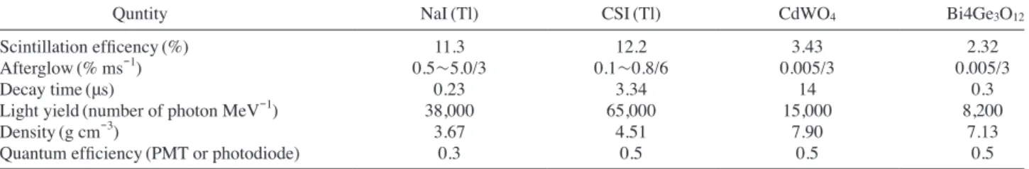
Table 1 presents properties of typical scintillator which can be used for the high energy X-ray system; NaI(Tl), CsI(Tl), CdWO4(CWO) and Bi4Ge3O12(BGO). NaI(Tl) and CsI(Tl) have advantages of high light yield and high scintillation efficiency but their large afterglow may induce a significant ghost effect in a fast linear scanner or a com-puted tomography. CWO and BGO have much higher Z number and density than NaI(Tl) and CSI(Tl) so they have advantages of high detection efficiency. In addition, they have a strong advantage of low afterglow. BGO seems to be the best scintillator material in terms of its scintillation properties but its price is relatively high and the light inten-sity of BGO is low and it is also seriously reduced when the temperature increases(Martz et al. 1990). CWO is a mate-rial of reasonable price and has the very good manufactur-ability. The decay time of CWO seems to be large(14μs) but still short enough to achieve the reasonable scan speed. Therefore CWO was finally chosen as the best scintillator for the proposed system. Each CWO channel detector is coated with a thin TiO2 reflector layers.
The proposed detector array was designed not only applica-ble to CT but also to the linear scanning applications. A mod-ule of the 48 channel CWO block array and its single channel dimension(pitch, width and length) are shown in Fig. 2(a) and(b). The pitch(p) of CWO arrays is typically a few mm
for a cargo container inspection system and about 1mm for high energy industrial CT. In this study, we set the pitch to be 0.4mm to observe the finer defects in heavy objects such as a void or cracks in automobile engines or missiles to accommo-date both the linear scanner and CT applications. The width(w) of CWO should be determined depending on the scan speed in a linear scanner which again depends on the specific appli-cation types. The linear scanning appliappli-cation requires a fast scan speed(~100mm sec-1) but the CT application requires a relatively low vertical scan speed(~10mm sec-1). In order to cover the both scan speed, we set the width as 1mm. The width of 1mm will be proper for the high scan speed in a linear scanner and for the adequate slice thickness for CT. Finally the thickness(t) of the CWO block should be care-fully determined for considering the X-ray energy spectrum produced from the electron-to-X-ray conversion target in a linear accelerator to be used. In this study, the energy of a linear accelerator was assumed to have a range from 6 to 15 MeV. Fig. 2(b) shows the dimensions of a CWO block in a module. For the precise determination, Monte Carlo sim-ulations were performed. First high-energy X-ray spectra from a tungsten target by accelerated electrons in a linear accelerator were calculated using MCNPX code. Accelerat-ed electron energies considerAccelerat-ed were 6, 9 and 15MeV. Then the detection efficiency of CWO depending on the X-ray energy was calculated. Finally the detector height was
de-table 1. Properties of typical scintillators for high energy scanner and CT
Quntity NaI(Tl) CSI(Tl) CdWO4 Bi4Ge3O12
Scintillation efficency(%)
Afterglow(% ms-1)
Decay time(μs)
Light yield(number of photon MeV-1)
Density(g cm-3)
Quantum efficiency(PMT or photodiode)
11.3 0.5~5.0/3 0.23 38,000 3.67 0.3 12.2 0.1~0.8/6 3.34 65,000 4.51 0.5 3.43 0.005/3 14 15,000 7.90 0.5 2.32 0.005/3 0.3 8,200 7.13 0.5
Fig. 2. (a) A single module of CWO block array composed of 48 channels, (b) The geometric variables in a CWO block. Z (a) (b) t X p w Y X-ray direction
termined in considering not only the X-ray energy but also the cost and manufacturability.
3. design of a Si PIn photodiode array of an LdAu The scintillation light from a CWO block is sensed by a silicon PIN photodiode coupled to the CWO block with an optical transparent epoxy. Though the absorption lengths of two wavelengths(470 and 540nm) of scintillation light from CWO are relatively short, we decided to use 600μm PIN photodiode rather thinner PIN diode because of its low noise properties due to smaller capacitance. As the intrinsic layer becomes large, the resistance increases linearly so low resistivity wafer is desirable.
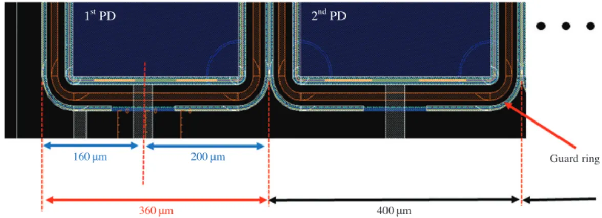
The photodiode array was designed as a module of 48 channels with the pitch of 400μm. The length of the pho-todiode is the same as the height of the CWO to be deter-mined. The first and the last photodiode channel has 40μm shorter than the pitch for wafer dicing margin and connect-ing margin to the next module when makconnect-ing a long linear detector array of the LDAU. The active area of a photodi-ode has a dimension of 0.3mm×17mm(area=5.1mm2) where the length is 0.3mm and is 0.1mm shorter than the pitch due to the guard rings. The detailed shape for the first and a middle photodiode is shown in Fig. 3. Double-lay-ered guard ring structure was also adopted to minimize leakage current which mainly flows through the surface of each layer. It also reduces the interference from outside of the system and the cross-talk between nearby channels. As shown in Fig. 3, every corner of active area and guard rings was designed to have a smooth curvature to avoid electrical breakdown due to the sharp edge.
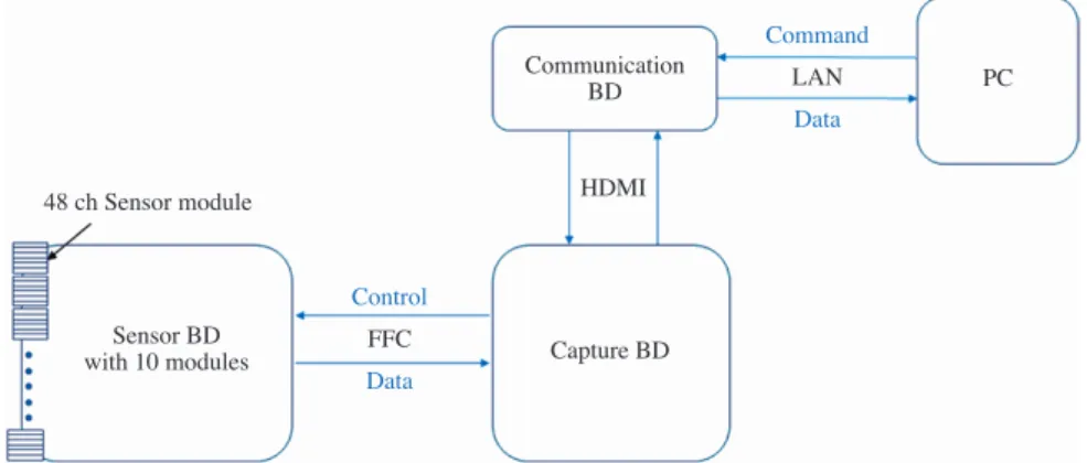
4. design of 3-board dAS for an LdAu
The data acquisition system(DAS) for a single LDAU was designed to be composed of three boards; a sensor board, a capture board and a communication board as shown in Fig. 4. The first board is a sensor board where the 10 modules of 48 channel CWO-PIN combinations will be inserted through a dual line socket and 480 channel signals will be sampled, preamplified(integrated) and digitized. The main component in this board is 64 DDC118 chips where dual current integrating preamplifiers per channel were adopted. For a given integration period, the feedback capacitor on the preamplifier integrates a signal current generated from the PIN diode. By using a dual-switched integrator at the input stage, there is no dead time of the de-tector because when a signal is integrated in a preamplifer, the other preamplifier signal is undergoing a digitization process. The acquired data were directly converted into 16-bit digital data. Daisy-chained serial data is transferred to a memory in the capture board, and then to the control con-sole in a PC. The DDC118 chips are controlled by a digital signal and a clock from the second board, a capture board. The connection between the sensor board and the capture board was made using 3 flat flexible cables(FFC).
The main function of the capture board is to produce var-ious control signals, clocks and dc powers which are nec-essary by the sensor board, and to capture the digital data from the sensor board to make a 2-D image, store them in a memory and send them to the communication board. The nominal format of the image was designed to be 480 chan-nel×512 lines. These image data and the control signals from the capture board and the third board, a communica-tion board, are transmitted via an HDMI(high definition
1st PD 2nd PD
160μm 200μm
360μm 400μm
Guard ring
Fig. 3. The partial layout of Silicon PIN photodiodes. The pitch of all photodiodes is 400μm except the first and the last photodiodes in a 48
Linear Detector Array Unit 149
multimedia interface) cable.
The third board was designed to transfer data to a PC through a LAN cable and it produces additional control signals for the external x-ray generator and the rotation and linear motion of the stage. The long LAN(local area net-work) cable will be useful for high energy X-ray system be-cause its control should be remotely done for the radiation safety of the operators.
reSuLtS
1. optimization of cWo detectors for 15MeV by Monte carlo simulation
In order to decide the height(h) of a CWO block for high energy X-ray generated from a linear accelerator, Monte
Carlo simulations were performed using a simplified geom-etry as shown in Fig. 5(a). A 0.4mm thick tungsten was as-sumed as a target to generate the high-energy X-ray from 6, 9 and 15MeV electrons and a 0.5mm thick lead filter was assumed to be placed at the beam direction to cut off the low-energy X-ray. The calculated X-ray energy spectrum by accelerated electron beam is shown in Fig. 5(b). From the simulated spectra, the mean energies of X-rays were calculated to be 0.988, 1.405, and 2.127MeV for 6, 9 and 15MeV electrons. These results are obtained with F5 point detector tally that is placed on the back of the tungsten target. In low energy region of Fig. 5(b), the characteristic X-ray energies from the tungsten target and lead filter are also found.
Because the mean energy of X-rays from a linear accel-erator with an electron energy of 6~15MeV was in the
48 ch Sensor module Capture BD PC Communication BD Control FFC Data Command LAN Data HDMI Sensor BD with 10 modules
Fig. 4. The block diagram of the data acquisition system(DAS) composed of a PC and 3 boards; a sensor board, a capture board and a com-munication board. Electron beam : 6~15MeV 1E-3 1E-4 1E-5 1E-6 1E-7 1E-8 Counts cm -2 (fluence) 15MeV electrons 9MeV electrons 6MeV electrons Target : Tungsten Collimator : Lead X-ray beam Filter : Lead 0 2 4 6 8 10 12 14 16 X-ray energy(MeV)
(a) (b)
Fig. 5. (a) The simplified geometry for Monte Carlo simulation of 6, 9 and 15MeV electrons in a linear accelerator,(b) the X-ray energy
order of 0.988~2.127MeV, we determined the optimum thickness of the detector from the response curve of 2MeV X-ray in Fig. 6. The saturation behavior of the detector response for the mean X-ray energy ranging from 2 to 10 MeV are shown. The finally determined optimum thickness of the CWO detector was 17mm. With this thickness, the absolute detection efficiency for high energy X-rays from a 15MeV linear accelerator was calculated as the ratio of the deposited energy to the mean energy and it was ~30% (=0.64MeV/2.0MeV) as shown in Fig. 6. The thickness larger than this would not bring any further advantage.
2. Fabrication and characterization of silicon PIn photodiodes
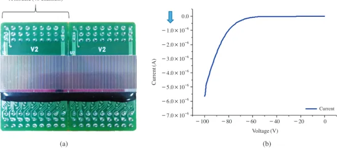
The PIN photodiodes grouped as modules were fabricat-ed at ETRI(Electronics and Telecommunication Research Institute, Daejeon, Korea) using N-type NTD(neutron trans-mutation doping) wafers with(100) orientation and sheet resistance of 125Ωcm. NTD wafers have been known to have a lower leakage current than the purified wafers(Park et al. 2006). Fig. 7(a) shows 2 modules of silicon PIN pho-todiodes assembled on a detector PCB. A PIN diode is usu-ally operated under a reverse bias condition but sometimes at zero bias condition. The mini detector PCB was designed for both with and without operation bias. Using a manual probe station, current-voltage measurement was performed with all bare chips. Among 48 channels of a typical mod-ule, one representative result of I-V measurement is given in Fig. 7(b). The leakage current was about 167pA at 3V, 850pA at 5V, and 5nA at 10V reverse biases. The reverse breakdown voltage was about 65V.
3. Fabrication of data acquisition system for an LdAu
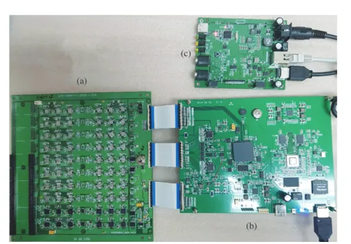
The data acquisition system(DAS) comprising three functional boards was fabricated and its picture is shown in Fig. 8. The capture board and the communication board were tested. The sensor board is under fabrication. When
A module(48 channels) Current (A) 0.0 -1.0×10⁻⁶ -2.0×10⁻⁶ -3.0×10⁻⁶ -4.0×10⁻⁶ -5.0×10⁻⁶ -6.0×10⁻⁶ -7.0×10⁻⁶ -100 -80 -60 -40 -20 0 Voltage(V) (a) (b) Current
Fig. 7. (a) Two Si PIN photodiode modules mounted on a detector PCB,(b) The measured current-voltage characteristics of fabricated
Sili-con PIN photodiode as a function of the reverse bias. The reverse leakage current is below 1nA at 5V and the breakdown voltage was
about 65Volt. Deposited ener gy in a CWO block (MeV) 0.0 2.5 5.0 7.5 10.0 12.5 15.0 17.5 20.0 22.5 CWO thickness, t(mm) 1.4 1.3 1.2 1.1 1.0 0.9 0.8 0.7 0.6 0.5 0.4 0.3 0.2 0.1 2MeV 4MeV 6MeV 8MeV 10MeV
Fig. 6. The detector response curve of a CWO block as a function
of the detector thickness for various mean X-ray energies
from 2 to 10MeV. The mean energy of 2MeV is equivalent
Linear Detector Array Unit 151
the capture board was tested to confirm its system integri-ty, no external synchronized timing was necessary. Fig. 9 shows the test results of pre-programmed image data from the DAS system without connecting the sensor board. The black and white area represent the dynamic range in the im-age.
dIScuSSIon
The decision of the CWO-PIN detector’s dimensions was made for the high energy X-ray helical CT based on a LINAC. The pitch of channels is 0.4mm for the high reso-lution. The width is 1mm for the high scan speed. Most im-portantly the optimum thickness of 17mm was determined for detecting the high energy X-rays from 6, 9 and 15MeV LINACs based on the MCNP simulations. The thickness larger than this would not bring any further advantage.
This thickness with ~30% detection efficiency will be high enough to get a good quality image from a LINAC of the electron energy up to 15MeV.
The 0.4mm pitch Si PIN photodiode was also designed and fabricated using N-type 125Ωcm NTD wafers. The active area length within this pitch is 0.3mm. The round-ed corner shape of the active region and the guard rings brought the low leakage current characteristics. The mea-sured leakage current level of less than 1nA at the opera-tion bias of 5V was obtained and it would be suitable for achieving the good signal-to-noise ratio for a 15MeV LIN-AC with a typical operation current levels.
The DAS for an LDAU was also designed and fabricated. Through a preliminarily test without connecting the sensor board, it wa proved that the DAS could be properly operat-ed for the field X-ray test. Presently the electro-optical and field X-ray test of the LDAU is under preparation.
concLuSIon
A linear detector array unit having 480 channels was de-signed and fabricated together with its data acquisition sys-tem. This unit can be used to form an arc shape detector in a high energy X-ray helical CT system for NDT of automo-bile engines and missiles etc. The detector is composed of 10 modules and each module has a 48 channel CWO block
Fig. 9. The pre-programmed test image of the capture board.
Fig. 8. The fabricated data acquisition system(DAS) composed of 3 boards; (a) a sensor board, (b) a capture board and (c) a communication board.
(a)
(c)
array and a die of 48 channel silicon PIN photodiodes. The pitch of 0.4mm was determined for high resolution, the width of 1mm for high scan speed in linear scanner and for the proper slice thickness for CT. Most importantly the thickness of 17mm is determined to detect X-ray beams from a 15MeV linear accelerator based on Monte Carlo simulations. The PIN photodiodes were fabricated from N-type NTD(neutron transmutation doping) wafers with (100) orientation and the sheet resistance of 125Ωcm. The PIN photodiode has a rounded corner shape for the active area of 5.1mm2 and double-layered guard rings to minimize the reverse leakage current. The measured leakage current at 5V reverse bias was lower than 1nA. The level of leak-age current seems to be quite satisfactory in considering the signal-to-noise ratio in detecting X-rays from a 15MeV LINAC. Also the data acquisition system was designed as 3 individual boards for easy manufacturing and maintenance; a sensor board, a capture board and a communication board. In conclusion, a linear detector array unit with CWO-PIN combinations and the 3-board data acquisition system was successfully designed and fabricated, and it can be used to form a larger helical CT system or a linear scanner simply by multiple copying and Daisy chaining.
AcKnoWLedgMent
This work was supported by the Korea Institute for Ad-vancement of Technology(KIAT) under the Ministry of
Trade, Industry and Energy(Project Serial Number: N000 1647).
reFerenceS
Butt A. 2014. A Review of Real Time Radiography as a s Solid Propellant Burn Rate Measurement Technique. AIAA Re-gion II Student Conference. Memphis, TN.
Martz HE, Azevedo SG, Brase JM, Waltjen KE and Schneberk DJ. 1990. Computed Tomography Systems and Their In-dustrial Applications. Int. J. Radiat. Appl. Instrum. Part A.
41(10):943-964.
Nikl M. 2006. Scintillation Detectors for X-rays. Meas. Sci.
Tech. 17(4):37-54.
Park KS, Park JM, Yoon YS, Koo JG, Kim BW, Yoon CJ and No KS. 2006. Effects of the Resistivity and Crystal Orien-tation of the Silicon PIN Detector on the Dark Current and Radiation Response Characteristics. IEEE Nuclear Science Symposium and Medical Imaging Conference. San Diego, USA.
Xiao Y, Chen Z, Li Y and Ye L. 2016. Development and Appli-cations of High Energy Industrial Computed Tomography in China. 19th World Conference on Non-Destructive
Test-ing. Munich, Germany.
Zentai G. 2011. Comparison of CMOS and a-Si Flat Panel Im-agers for X-ray Imaging. IEEE International Conference on Imaging Systems and Techniques. Palo Alto, CA.
Received: 19 August 2016 Revised: 9 September 2016 Revision accepted: 12 September 2016