22-3 / S. Lamansky
• IMID 2009 DIGEST
Abstract
Nanostructured OLED light extraction films have been made via roll-to-roll coating processes. Their on-axis and integrated outcoupling efficiencies reach 2X and 1.3-1.8X, respectively. Optical performance and effects of the nanostructured film on pixel blur and image ghosting will be discussed.
1. Introduction
External efficiency of organic light emitting devices (OLEDs) is a critical parameter for all OLED applications ranging from high-resolution displays to lighting, since it influences important device characteristics such as power consumption, luminance and lifetime. It has been demonstrated by a number of groups that OLED external efficiency is greatly limited by optical losses within the OLED stack itself. These include unextracted waveguide modes within the high-index organic layers and indium tin oxide, and within typical substrates [1]. Additional losses may originate upon exciton quenching at metal electrode surfaces. In a device with a maximum possible internal efficiency (100% internal), about 75-80% of this efficiency is dissipated internally due to above-mentioned losses. Among the variety of approaches that have been proposed for addressing the OLED optical losses and improving OLED light extraction, the most prominent ones include external or internal scattering layers based on random arrays of scatterers, internal regular photonic crystal structures, special high-index substrates, low-index OLED materials, microcavities, and special patterns at the organic/metal electrode interface [2] .
3M has been developing a film-based OLED light extraction solution based on roll-to-roll fabricated nanostructures. The nanostructures are
capable of redirecting light which is tightly confined within high-index organic layers or undergoing total internal reflection within the OLED substrates. In this paper, we report on both random and regular nanostructures which are incorporated between layers of large refractive index contrast within the OLED device stack to improve device light outcoupling efficiency.
2. Experimental
Nanostructured light extraction films were fabricated in a roll-to-roll process, details of which have been discussed elsewhere [3].
Green, Red and Blue bottom-emissive OLEDs with general architecture ITO/HIL/HTL/EML/ETL/ /cathode were fabricated on the nanostructured light extraction films and control glass and film substrates at standard vacuum deposition conditions at base pressure of ca. 10-6 torr.
Electrical and optical performance of resulting OLEDs was evaluated in a number of ways, using PR650 camera coupled to Keithley2400 Sourcemeter for on-axis LIV, EL spectra and goniometric tests, and using ConoScope-80TM (Autronic Melchers GmbH,
Germany) for conoscopic angular measurements.
3. Results and discussion
A typical light extraction structure as applied to the bottom-emissive OLED stacks reported herein includes the nanostructured layer at the interface between the indium-tin oxide (nITO ~ 2.1) and
OLED Light Enhancement with Nanostructured Films
Sergey Lamansky*, Ha Le, Encai Hao, David Stegall, Ding Wang, Yi Lu,
Jun-Ying Zhang, Terry L.Smith, Mark Gardiner, Leslie Kreilich,
Jonathan Anim-Addo, and Fred B.McCormick
3M Display and Graphics Business Laboratory and Corporate Research Laboratory 3M Company, Saint Paul, MN 55144, USA
Tel.: 1-651-737-4876, E-mail: [email protected]
22-3 / S. Lamansky IMID 2009 DIGEST • sample number re la tiv e p eak ef fici en cy , a .u . 17 16 15 14 13 12 11 10 9 8 7 6 5 4 3 2 1 2.5 2.0 1.5 1.0 0.5 control pixels nanostructured pixels a sample number vo lta ge a t 20 m A/ cm2 , V 17 16 15 14 13 12 11 10 9 8 7 6 5 4 3 2 1 14 12 10 8 6 4 2 0 control pixels nanostructured pixels b sample number re la tiv e p eak ef fici en cy , a. u. 10 9 8 7 6 5 4 3 2 1 2.5 2.0 1.5 1.0 0.5 control pixels nanostructured pixels c sample number Vo lta ge a t 20m A/ cm 2, V 10 9 8 7 6 5 4 3 2 1 14 12 10 8 6 4 2 0 control pixels nanostructured pixels d
Figure 1. a. Relative on-axis efficiency and b. voltage at 20mA/cm2 for green OLEDs made with conformal high-index coatings, and c. relative on-axis efficiency and d. voltage at 20mA/cm2 for green OLEDs made with high-index coatings.
substrate (nS ~ 1.4-1.5). Previous studies have
concluded that modulating the refractive index in the nanostructured layer is critically important for efficient light outcoupling enhancement.
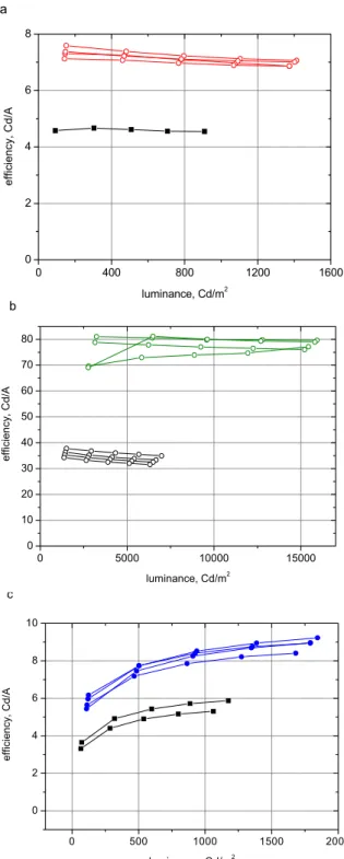
0 400 800 1200 1600 0 2 4 6 8 a ef ficiency , Cd/A luminance, Cd/m2 0 5000 10000 15000 0 10 20 30 40 50 60 70 80 b effic iency , Cd/ A luminance, Cd/m2 0 500 1000 1500 2000 0 2 4 6 8 10 c e ff ici en cy , Cd /A luminance, Cd/m2
Figure 2. On-axis efficiency of a. red, b. green and c. blue OLEDs on nanostructured films.
22-3 / S. Lamansky
• IMID 2009 DIGEST
Our studies indicate that it is also essential to induce adequate planarization over the nanostructures prior to electrode deposition. The planarization cannot be accomplished with conventional high-index materials such as SixNy commonly deposited via a
plasma-enhanced chemical vapor deposition (PECVD) process due to the conformal nature of the coatings. Morphological non-uniformities resulting from conformal high-index coatings may lead to undesirable variations in the current-voltage behavior of OLEDs [4]. Figure 1 compares the statistics of relative OLED efficiency and voltage data for a set of nanostructures overcoated with a conformal a index material (Figure 1a,b) and a planarizing high-index material developed in our laboratory (Figure 1c,d).
a.
b.
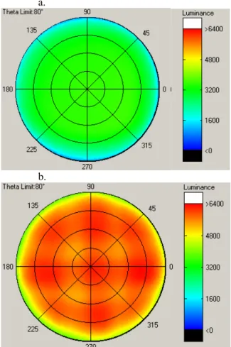
Figure 3. Angular luminance distributions of green OLEDs fabricated on a. control and b. nano-structured filmsubstrates.
Efficiency data for each OLED sample was normalized to the efficiency of a corresponding control pixel which was prepared without the light extraction nanostructure. Figures 1a and 1b show that
with the conformal high-index coating, significant variability is observed both in optical and electrical characteristics of the devices. Such variability is reduced dramatically upon introducing the planarizing material (Figure 1c,d); moreover, larger average efficiency enhancement is observed with the planarizing material.
On-axis efficiency enhancement for green (λEL = 510nm), blue (λEL = 460nm) and red (λEL =
620nm) OLED constructions built on top of identical nanostructured films planarized with the high-index material is illustrated in Figure 2. Up to 1.7X, 2.2X and 1.7X outcoupling enhancement is observed with the nanostructured film for red, green and blue OLEDs, respectively, compared to the control devices made without the nanostructures, thus demonstrating the broadband effectiveness of this approach.
a.
b.
Figure 4. Pixel blur effects of the 70um wide OLED line-wise pattern with a. external microlens films and b. nanostructured film.
Analysis of the far-field emission reveals pattern-wise but fairly uniform angular luminance distribution (see Figure 3). It should be noted that angular luminance distributions with the
22-3 / S. Lamansky
IMID 2009 DIGEST • nanostructured films depend on the magnitude of
microcavity effects pre-built into OLED stacks as well as to some extent on spectral emission characteristics.
OLED light extraction solutions dealing with optical losses due to total internal reflection such as microlenses, brightness enhancement films and microprisms have been shown to have limited applicability to high-resolution displays because of substantial pixel blur effects [5]. We have mimicked a monochrome high-resolution OLED pattern by proving high-resolution patterning of indium-tin oxide anode, and studied the effects of both external lenticular films prepared at 3M as well as effect of nanostructured films onto pixel blur (Figure 4). Figure 4 shows that, while external microlens films cause complete blurring of the 70um wide line-wise OLED pattern, with the nanostructured film the pattern is preserved.
4. Summary
Practical application of the light extraction film in displays and lighting products requires the film to be compatible with existing or developmental OLED manufacturing processes, materials, and device architectures. It also imposes a need for a low-cost manufacturing solution for the film itself, dictating development of continuous web coating and nanostructuring solutions. We believe the film approach may be a viable alternative for OLED outcoupling not only for low-resolution and lighting applications, but for high-resolution displays as well.
Acknowledgement
The authors would like to acknowledge Kenneth Looney, David Lawrence, Katie Rufener, Martin Wolk, Melvin Zin, Olester Benson, and Blake Kolb, all of 3M Company, for assistance with various aspect of the project.
5. References
[1] a. M-H.Lu et al., J. Appl. Phys. 2002, 91(2), 595; b. J.Revelli et al., Appl. Optics 2005, 44(16), 3224 [2] a. R.Bathelt et al., Org.Electr. 2007, 8, 293, b. H.
Greiner Jap. J. Appl. Phys. 2007, 46(7A), 4125; c. A.Werner et al., SID 2008, Paper 36.5, May 23-27, Los Angeles, California; d. P.A.Hobson et al. , IEEE
J.Selected Topics in Quantum Electr. 2002, 8(2), 378; d. T.Nakamura et al., J. Appl. Phys. 2005, 97, 054505; e. T.Nakamura et al., J. Appl. Phys. 2004, 96(11), 6016; f. T.Tsutsui et al., Appl. Phys. Lett.
1994, 65(15), 1868; g. R.H. Jordan et al., Appl.
Phys. Lett. 1996, 69(14), 1997
[3] S.Lamansky et al., International Display Research Conference 2008, Orlando, FL
[4] a. M.Fujita et al., Appl.Phys.Lett. 2004, 85(23), 5769; b. Y.R.Do et al., Adv. Mater. 2003, 15(14), 1214