저작자표시-비영리-변경금지 2.0 대한민국 이용자는 아래의 조건을 따르는 경우에 한하여 자유롭게
l 이 저작물을 복제, 배포, 전송, 전시, 공연 및 방송할 수 있습니다. 다음과 같은 조건을 따라야 합니다:
l 귀하는, 이 저작물의 재이용이나 배포의 경우, 이 저작물에 적용된 이용허락조건 을 명확하게 나타내어야 합니다.
l 저작권자로부터 별도의 허가를 받으면 이러한 조건들은 적용되지 않습니다.
저작권법에 따른 이용자의 권리는 위의 내용에 의하여 영향을 받지 않습니다. 이것은 이용허락규약(Legal Code)을 이해하기 쉽게 요약한 것입니다.
Disclaimer
저작자표시. 귀하는 원저작자를 표시하여야 합니다.
비영리. 귀하는 이 저작물을 영리 목적으로 이용할 수 없습니다.
변경금지. 귀하는 이 저작물을 개작, 변형 또는 가공할 수 없습니다.
Jeonghyeon Kim
Department of Electrical Engineering
Ulsan National Institute of Science and Technology
Ferroelectric Nonvolatile Memory Based on Two- Dimensional van der Waals CuInP 2 S 6 and WSe 2
Heterojunction
Abstract
Ferroelectric non-volatile memory has been extensively investigated due to the promising properties such as low-voltage and low-power consumption. However, the integration of 3D ferroelectric insulator with 2D semiconductor leads to interface traps which are responsible for Vth shift. [1] The use of 2D ferroelectric materials for 2D semiconductor can be a solution to this problem.
In order to analytically understand the electrical characteristics of Si-based ferroelectric field-effect transistor (FeFET), mathematical models have been suggested by Miller et al. [2]. Meanwhile, two- dimensional (2D) transition metal dichalcogenides (TMDCs) have emerged as a promising channel material in ultra-scaled FET due to the atomically thin nature. Accordingly, there have been several experimental demonstrations of FeFET with 2D channel material (2D FeFET), but little development of analytical models of 2D FeFET.
First, we present analytical models of 2D FeFET which are developed by modifying Miller’s FeFET model using the Poisson equation [3,4]. In order to obtain the channel charge in 2D TMDCs, Ward- Dutton charge partitioning method adopted by Jiang et al [3] is used. To explain FeFET behavior more precisely, the mathematical model to describe the non-saturated hysteresis loop of ferroelectrics is adopted [5]. We consider Metal-Ferroelectric-Insulator-Semiconductor (MFIS) structure for 2D FeFET which could be constructed using CuInP2S6 (CIPS), h-BN and WSe2 as 2D ferroelectric, 2D insulator and 2D channel materials, respectively. Models for 2D FET without ferroelectrics are also presented to be compared with 2D FeFET and clarify how 2D FeFET works. We study the dependency of memory window in 2D FeFET on the ferroelectric properties (remnant polarization Pr and coercive field Ec), thickness and dielectric constant of ferroelectric and insulator. Consequently, our work aims to present the optimized 2D FeFET structure that can maximize the memory window.
Second, we report 2D ferroelectric van der Waals heterostructures (vdWHs) IV characteristics and memory reliability characteristics composed of potentiation-depression (PD) curve and retention property. The 2D ferroelectric vdWHs are constructed stacking WSe2, hBN and CIPS through the dry transfer method. The devices demonstrate hysteric transfer characteristics with a large memory window, large on/off ratio (107) and small gate leakage current (10-12 A). Also, memory reliability is validated showing endurance property with PD curve consisting of 10 cycles where each cycle is composed of 32 potentiation and 32 depression pulses and retention property with program and erase state being maintained for 1000 s.
Contents
Ⅰ. Introduction ---1
1.1. Two-dimensional Transition Metal Dichalcogenides---1
1.2. Ferroelectric Field Effect Transistor---2
1.3.Multilevel state and Memory reliability---4
Ⅱ. Analytical Modeling of 2D Ferroelectric Field Effect Transistor ---5
2.1. Modeling Approach ---5
2.2. 2D FET vs. 2D FeFET Modeling IV characteristics ---10
2.3. Thickness Dependent Memory Window & On current of 2D FeFET Modeling---11
Ⅲ 2D FeFET with CIPS and WSe2 Heterojunction---13
3.1. Device Fabrication---13
3.2. Device characteristics of CIPS/h-BN/WSe2 FeFET with Top and Back gate ---14
3.3. Device characteristics of CIPS/h-BN/WSe2 FeFET and h-BN/WSe2 with bottom gate---16
3.4. Device characteristics of CIPS/h-BN/WSe2 FeFET and CIPS/WSe2 with bottom gate---19
3.5. Memory reliabilities of CIPS/h-BN/WSe2 FeFET device ---20
Ⅳ. Conclusion ---22
1
1. Introduction
1.1. Two-dimensional Transition Metal Dichalcogenides
Figure 1. Three-dimensional MoS2 structure [6] Figure 2. Monolayer MoS2 transistor [6]
Two-dimensional transition metal dichalcogenides (2D TMDCs) are attracting considerable interest because downscaling the physical size of silicon-based conventional MOSFET is approaching its limit [1], [6]-[9]. Bulk TMDCs are vertically stacked, weakly bonded each layer by van der Waals interactions so single layer of TMDC can be gained using mechanical exfoliation such as scotch tape or lithium-based intercalation [10], [11]. Despite the fact that graphene is generally known to have zero band gap, 2D TMDCs have a suitable band gap (1~2 eV), making them upcoming electronic devices with high Ion/Ioff ratios. In addition, TMDCs have thickness-dependent electronic band structure, for example, bulk MoS2 has a 1.2 eV indirect band gap, whereas monolayer (~6.5 Å) MoS2 has a 1.8 eV direct band gap [6].
Most of TMDCs could have potential to be adopted as high performance device applications fabricating heterojunction or homojunction devices due to remarkable properties for example, dynamically gate-tunable behaviors and dangling bond-free [12].
Commonly, MoS2 is often taken as TMD-based n-FET owing to surprising electron mobility up to 700 cm2V-1s-1, high Ion/Ioff ratio (~108), optical transparency, mechanical flexibility, tunable band-gaps by engineering the number of layers and thermal stability up to 1100 ℃ [6], [10]-[14].
It is also important to look into TMD-based p-FET in order to utilize TMDCs in the CMOS architecture.
MoTe2, 2D black phosphorus (BP) and WSe2 have been investigated to present p-type conduction but MoTe2 and BP are unstable in ambient conditions. In contrast, WSe2 shows a high environmental stability and hole mobility approaching 500 cm2V-1s-1 [15]-[17].
Herein, our work adopted WSe2 as a channel material to explore p-type FeFET because several n-type FeFETs have been reported already.
2
1.2. Ferroelectric material
Figure 3. Crystal sturcuture of CIPS, Top view (a), side view (b), AFM image (c) and height profile (d) [18]
Figure 4. Hysteresis loop of Polarization-Electric field (P-E) curve
Ferroelectricity is a feature of some materials, which is a spontaneous electrical polarization of ionic displacement under an external electric field. The direction of dipoles point randomly in a ferroelectric material at no external electric field, but the dipoles align with the field when an adequate strong field, i.e., the coercive field is applied. Even if the field is removed, the dipole alignment remains so the polarization of the dipoles is kept permanently. This permanent polarization is called as a remnant polarization (Pr), which are the intrinsic properties of ferroelectric material. In order to remove or change the direction of dipole alignment, a properly strong field should be applied in the opposite direction. This polarization change with respect to an external electric field presents the closed loop known as hysteresis meaning that the material remembers what has happened to it before. Also, Franz Priesach developed the purely mathematical model of hysteresis for ferroelectricity and ferromagnetism describing ferroelectrics as an assembly of independent hysterons [19]. Furthermore, Miller et al. have
3
developed this Preisach model and suggested an analytical model of FeFET in order to mathematically examine the electrical characteristics FeFET [2].
Perovskite oxides with strong covalent or ionic bonds are commonly investigated types of ferroelectrics for instance PbTiO3, BaTiO3, PbZrO3 and Pb[ZrxTi1-x]O3 (PZT) etc. However, the three- dimensional structure of perovskite oxide needs careful selection of substrate and epitaxial growth due to dangling bonds and defects at the interface between ferroelectric and substrate [20].
Within this mind, two-dimensional layered ferroelectrics are recently emerged such as α-InSe, CuInP2S6 and SnTe due to no dangling bond or defects, which implies enhanced device performances.
Also, thinner 2D layer builds smaller coercive field so lower power consumed device might be anticipated with 2D layered ferroelectrics [21]. Hence, we integrated 2D layered CIPS as a ferroelectric of FeFET expecting higher device performance.
4
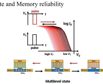
1.3. Multilevel state and Memory reliability
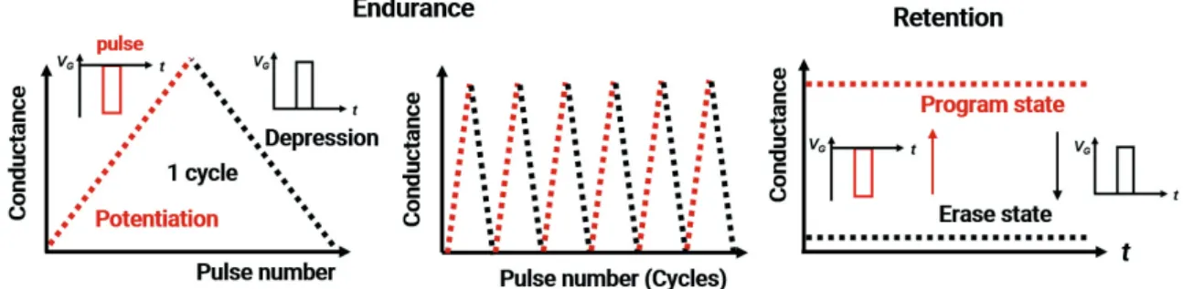
Figure 5. Multilevel states of ferroelectric memory which can converted by positive or negative pulses
As shown as Fig. 5, the threshold voltage (VT) of a ferroelectric field effect transistor can be changed gradually if the memory window is considerably broad. The reason why it is possible is due to the partial polarization of the ferroelectric material. It draws or pulls the charge in the channel partially. If external pulses are applied at the gate so as to switch the polarization in a non-volatile manner, the VT
can be tuned. This gradually controlled VT state is called as multilevel state, which can store several data [22].
Figure 6. Memory reliability (endurance and retention which can controlled by the pulses)
The multilevel state of a ferroelectric field effect transistor can be used to mimic the weighted synaptic, which can compose neuromorphic systems [22]. Also, the performances are examined as the memory reliability: endurance and retention. Endurance consists of both potentiation and depression. Applying the same pulses continuously at the transistor, the procedure is called as potentiation if the conductance is enhanced, on the contrary, that is called as depression if the conductance is reduced. One cycle is composed of a potentiation and a depression. If the device still keeps the conductance level even some degradation after undergoing several cycles, the endurance of the device might be guaranteed. In the same manner, after applying the pulse the device, if the conductance is maintained steadily as time goes, retention of the device might be guaranteed. The commonly accepted guaranteed period as a non- volatile memory application is approximately 10 years [22, 23].
5
2. Analytical Modeling of 2D Ferroelectric field effect transistor 2.1. Modeling Approach
Prior to 2D FeFET fabrication, to optimize the structure and parameters of 2D FeFET, a theoretical understanding of the relationship between the parameters of materials and the electrical properties. In order to analytically understand the electrical characteristics of silicon based ferroelectric field-effect transistor, mathematical models have been studied by Miller et al. [2]. However, there has been little development of analytical models to describe 2D FeFET. As shown in Fig.8, we present analytical models of 2D FeFET which are developed by modifying Miller’s FeFET model using the Poisson equation, Pao-Sah integral current, Ward-Dutton charge partitioning method and Preisach model of hysteresis of ferroelectric material
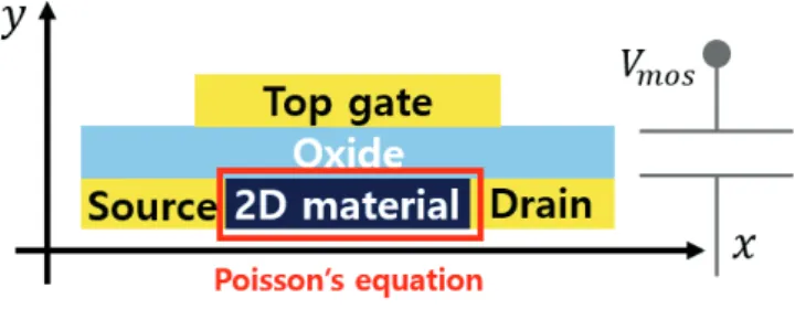
Figure 7. Schematic structure of 2D FET with the capacitance of oxide applied Vmos.
So as to account for analytical model of 2D FeFET, 2D FET model which excludes the ferroelectric material should be considered at first. Subsequently, 2D FeFET model where the ferroelectric material is inserted between the top gate and the oxide can be explained by combining Preisach model of the ferroelectric capacitor and 2D FET model. As illustrated in Fig. 7, the physical model of 2D FET considers only x and y axis in order to describe VDS and VGS, respectively. The equations are developed as below if the Poisson’s equation is applied to 2D FET model. The electric potential of 2D material, Ԅ is the function of x and y, so the Poisson equation is described as
݀ଶ߶
݀ଶݔെ݀ଶ߶
݀ଶݕ ൌݍሺ݊ଶെ ܰௗሻ ߝଶݐଶ
(1)
where
݊ଶൎ ܰଶή ൬ݍሺ߶ሺݔǡ ݕሻ െ ܸ
݇ܶ ൰ (2)
ܰଶ ؠ݉כ݇ܶ ʹߨଶ
(3)
6
In Eqs. (1), (2) and (3), q is the electron charge, n2D is the electron density per unit area in the channel, Nd is the areal doping concentration in the channel, and Vch is the channel quasi-Fermi potential, indicating the potential difference between at the source and the drain [4]. Due to ultrathin 2D material channel, the electrostatic potential may be considered uniform along the y axis. Hence, when the Gauss’s law is taken into the potential along the y axis, the left side of Eq. (1) could be transformed as below
݀ଶ߶
݀ଶݔെ ߶
ߣଶ ߦ ൌݍሺ݊ଶെ ܰௗሻ ߝଶݐଶ
(4)
where
ߦ ൌ ሺܸ௦െ ܸிሻ ߣଶ
(5)
ߣ ൌ ඨߝଶݐଶݐ௫ ߝ௫
(6)
In Eqs. (5) and (6), Vmos is the top gate bias, and VFB is the flat band voltage, meaning the work function difference between the gate and the channel when the source and the drain are grounded.
Comparing the length with the thickness of the channel, the second derivative of the potential ϕ with respect to x is much smaller than other terms in the left side of Eq. (4). Thus, when Eq. (4) is substituted into Eq. (2), the potential of the channel can be found without derivative form
߶ሺݔሻ ൌ ܸ݇ܶ
ݍ ݈݊ ൜ߝʹܦݐʹܦ
ݍܰଶߦ െ߶ሺݔሻ ߣʹ ൨ ܰ݀
ܰʹܦൠ (7)
Lambert function method, where W0(x)෭exp [W0(x)] = x, should be used to solve Eq. (7), so rearranging the terms of the variables in Eq. (7) as below
߶ሺݔሻ ൌܾ
ܽെ݇ܶ
ݍ ܹ൬ ݍ
ܽ݇ܶ݁ݔ ݍሺܾ െ ܸܽሻ
ܽ݇ܶ ൨൰ (8)
where
ܽ ൌ ߝଶݐଶ
ݍܰଶߣଶ
(9)
ܾ ൌ
ቀߝଶݐଶߦ ݍ ܰௗቁ
ܰଶ
(10)
7
Using the Pao-Sah integral current formulation, the drain current, IDS can be described with the source- drain voltage, VDS as
ܫௌ ൌ ߤ݊ݍܹ
ܮ න ݊ଶ
ವೄ
ܸ݀ൌ ߤ݊ݍܹ
ܮ න ܰௗߝଶݐଶ
ݍ ൨ ݀߶ܸ݀
݀߶
ವೄ
(11)
which can be written as a function of the channel potential Ԅǡ
ܫௌ ൌ ߤ݊ݍܹ
ܮ ቈ൬ߝଶݐଶ
ݍ ൬ߦ ݇ܶ
ݍߣଶ൰ ܰௗ൰ ߶ െߝଶݐଶ
ݍߣଶ
߶ଶ ʹ
థೞ
థ (12)
where Ɋ is the effective electron mobility, W is the gate width and L is the gate length.
Therefore, if the gate voltage, Vmos and the source-drain voltage, VDS are known, the drain current IDS
in the 2D channel can be found by utilizing Eqs. (5), (8), (9), (10) and (12).
For 2D FeFET model shown in Fig. 8, the ferroelectric material is inserted between the top gate and the oxide so the ferroelectric capacitor should be considered due to the induced electric field in the ferroelectric material. As the gate voltage is applied, the voltage drop in the ferroelectric induces additional the gate voltage, so it draws more charge in the channel than in the case of 2D FET. In this view, we deduce the induced voltage in the ferroelectric material using Ward-Dutton charge partitioning method from the channel potential and Preisach model for polarization-electric field (P-E) relationship.
Figure 8. Schematic structure of 2D FeFET with the capacitances applied Vmos,VF, and VGS.
From the channel potential, the intrinsic channel charges (Qch) can be calculated by using Ward- Dutton charge partitioning method [4] as below
ܳൌ ݍܹ න ሺ
݊ଶെ ܰௗሻ݀ݔ ൌ ݍܹ න ሺ
݊ଶെ ܰௗሻ݀߶ሺݔሻ ݀ݔ
݀߶ሺݔሻ
(13)
As we mentioned before, the polarization of the ferroelectric material draws the charge in the 2D
8
channel, Qch, so we combine the polarization of ferroelectric with the channel charge. Subsequently, the voltage drop in the ferroelectric material may be found as a form of the electric field.
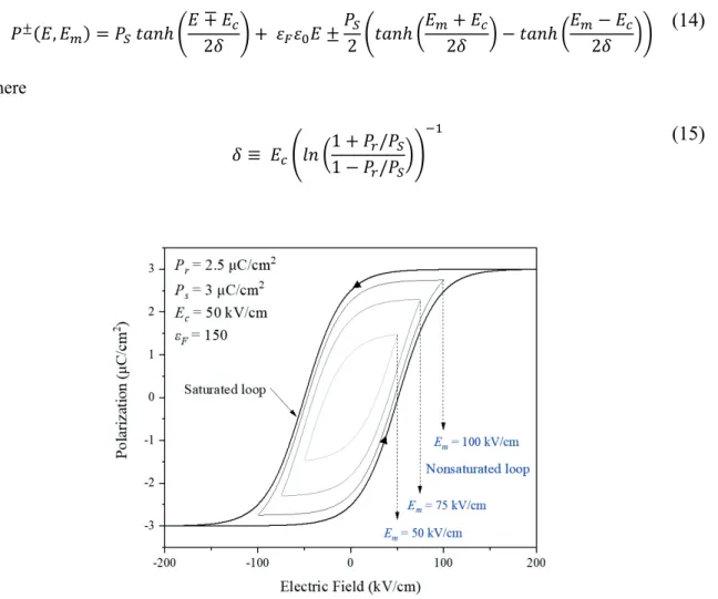
The modified Preisach model [5] for P-E relationship is written as
ܲേሺܧǡ ܧሻ ൌ ܲௌݐ݄ܽ݊ ቆܧ ט ܧ
ʹߜ ቇ ߝிߝܧ േܲௌ
ʹ ቆݐ݄ܽ݊ ൬ܧ ܧ
ʹߜ ൰ െ ݐ݄ܽ݊ ൬ܧെ ܧ
ʹߜ ൰ቇ (14)
where
ߜ ؠ ܧ൭݈݊ ൬ͳ ܲȀܲௌ ͳ െ ܲȀܲௌ൰൱
ିଵ (15)
Figure 9. Polarization-Electric Field curve for the ferroelectric material under several maximum electric fields, Em
Here, P+ indicates the positive-going branch of the hysteresis loop of P-E curve depicted in Fig. 9, while P- is the negative-going branch. Ps means the spontaneous polarization, Pr means the remanent polarization and Ec means the coercive field, where the parameters are the intrinsic properties of the ferroelectric material. Also, the first term in the right side of Eq.(14) denotes only retarded polarization when sweeping the electric field, and the second term ߝிߝܧ stands for the contribution of the dipole moment to polarization. The last term represents more complicated contribution to polarization of ferroelectric material and is used to express the minor hysteresis loop (nonsaturated situation). To describe more detail about minor loop, LUE et al. [5] suggested the concept of the polarization as a function of the maximum electric field, Em, which the ferroelectric material can be applied to, and it is given by
9
ܲௗሺܧሻ ൌ ߝிߝܧേܲௌ
ʹ ቆݐ݄ܽ݊ ൬ܧ ܧ
ʹߜ ൰ െ ݐ݄ܽ݊ ൬ܧെ ܧ
ʹߜ ൰ቇ (16)
As the applied voltage is increased, the dipole moment would go with ܲௗሺܧሻ until maximum electric field Em is get to. The reason why we construct the minor loop concept is that the polarization quite depends on the maximum electric field which the ferroelectric material undergoes as shown in Fig. 9.
Combining the modified Preisach model for P-E hysteresis loop with the 2D channel charge as a form of ܲേሺܧிǡ ܧሻ ൌ ܳ, the electrical field applied along the ferroelectric, EF is determined for a given channel charge, ܳ. Using EF, we can obtain the voltage drop in the ferroelectric VF, which is added to Vmos to get the final VGS in 2D FeFET as shown below:
ܸீௌൌ ܸ௦ ܸிൌ ܸ௦ ܧிݐி (17)
In summary, as the values of Vmos and VDS are given, the channel potential, ϕ is determined by Eq. (8) to solve for the 2D channel charge, ܳ and the drain current, ܫௌ by Ward-Dutton charge partitioning method and Pao-Sah integral current equation corresponding Eqs. (12) and (13), respectively. Since the polarization of the ferroelectric material draws the channel charge, the electric field in the ferroelectric layer EF can be obtained by assuming that the polarization is same with the channel charge. Therefore, given Vmos and VDS, the total gate voltage VGS is also obtainable with the drain current so we can determine the IDS – VGS plot by changing the gate voltage from 0 to VGS at the certain drain voltage VDS. The simpler modeling flow of 2D FeFET is shown as below in Fig. 10.
Figure 10. Modeling Flow of 2D FeFET with the schematic 2D FeFET structure.
10
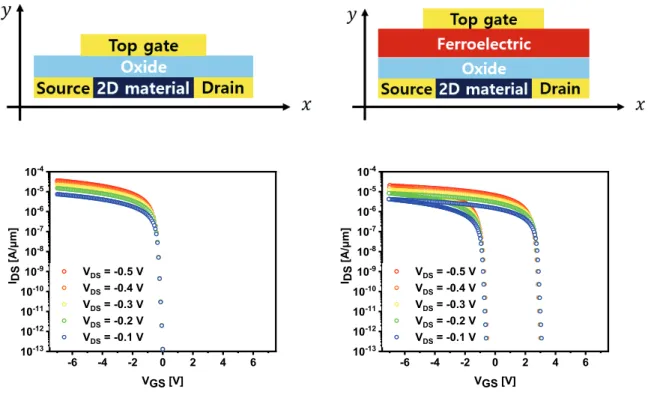
2.2. 2D FET vs. 2D FeFET Modeling IV characteristics
-6 -4 -2 0 2 4 6
10-13 10-12 10-11 10-10 10-9 10-8 10-7 10-6 10-5 10-4
I DS
[A/μm]
VGS [V]
VDS = -0.5 V VDS = -0.4 V VDS = -0.3 V VDS = -0.2 V VDS = -0.1 V
-6 -4 -2 0 2 4 6
10-13 10-12 10-11 10-10 10-9 10-8 10-7 10-6 10-5 10-4
I DS
[A/μm]
VGS [V]
VDS = -0.5 V VDS = -0.4 V VDS = -0.3 V VDS = -0.2 V VDS = -0.1 V
Figure 11. Schematic structures of 2D FET and 2D FeFET with transfer IV curves
On the left side in Fig. 11, using our models of 2D FET, we calculated IV of 2D FET composed of WSe2 and h-BN as 2D channel and oxide material. The right side is for 2D FeFET where we have CIPS, WSe2 and h-BN as the ferroelectric, 2D channel and oxide material, respectively. It can be clearly seen that the currents are modified from left to the right by the effect of ferroelectric in CIPS, which yields a memory window more than 2V. The parameter information: h-BN (t = 17 nm, ε = 3.29), CIPS (t =50 nm, ε = 5.29, Pr = 8 μC/cm2, Ps = 8.05 μC/cm2, Ec = 1400 kV/cm), WSe2 (t = 4 nm, ε = 5.16) [1,18,24,25].
11
2.3. Thickness Dependent Memory Window & On current in 2D FeFET Modeling
Using our 2D FeFET model, we explore the dependency of memory window on ferroelectric and oxide thickness. We set the thickness range from 10 nm to 50 nm of the both. The decrease of oxide thickness induces the increase of memory window and the increase of ferroelectric thickness induces the increase of memory window shown as Fig.12. The decrease of oxide thickness and the increase of ferroelectric thickness cause the decrease of ferroelectric capacitance, which means the increase of the voltage along the ferroelectric. As a result, it causes a larger memory window.
On the other hands, on current in 2D FeFET is also dependent of the thicknesses. The decrease of oxide thickness induces larger on current and the decrease of ferroelectric thickness also induces larger on current shown as Fig.13. Because the decrease of the thicknesses of ferroelectric and the oxide cause the increase of the total capacitance. It makes the on current large.
Depending on the thickness of ferroelectric material, memory window and on current would be fluctuated. In order to make the optimized ferroelectric memory, memory window should be expanded and on current should be enhanced. Therefore, the appropriate thickness of ferroelectric is required when fabricating the device due to the trade-off relationship between memory window and on current.
Figure 12. On current as a function of thickness of oxide and thickness of ferroelectric material
12
Figure 13. Memory window as a function of thickness of oxide and thickness of ferroelectric material
13
3. 2D FeFET with CuInP
2S
6and WSe
2Heterojunction 3.1. Device Fabrication
Local bottom gates (Cr/Au 2/8 nm) were fabricated using electron-beam lithography and electron- beam evaporation on a highly p-doped silicon substrate with 100 nm SiO2. To enhance the adhesion between the metal surface and the flakes and to remove surface strains, acetone cleaning was carried out. Subsequently, piranha cleaning was conducted with the mixed solution of hydrogen peroxide (H2O2) and sulfuric acid (H2SO4) (1:1).
Bulk CIPS, h-BN, and WSe2 were exfoliated onto the 100 nm SiO2 substrate using scotch tape dry exfoliation. The flakes with proper thickness and size, which was simply identified via optical contrast, were selected as the target flakes.
Each target flake was picked up at 40 ℃ and subsequently released over 70 ℃ using the polymer stamp, consisting of a stack of glass, a piece of polydimethylsiloxane and a polycarbonate film, under transfer stage with optical microscope. After each flake transfer, baking at 110 ℃ for 10 min and acetone cleaning for 30 min to remove the organic residue and to enhance the adhesion between flakes.
A number of electrodes and contact pads connected to the local bottom gate were patterned via electron-beam lithography. Subsequently, the WSe2 flakes were etched by oxygen plasma treatment to remove the organic residue. And then, Ti/Au (10/50 nm) electrodes and contact pads were deposited by electron beam evaporation.
Finally, in order to improve the interface problem such as defect states and to remove hydroxy group, formed due to humidity, on the WSe2 surface, post annealing was conducted at 250 ℃ for 2 hrs in a vacuum chamber at pressure of 1E-5 torr.
14
3.2. Device characteristics of CIPS/h-BN/WSe
2FeFET with Top and Back gate
Figure 14. (a) Schematic, (b) AFM image and (c) optical micrograph of the device structure. (d) Transfer IV curve with top gate voltage VGS. (e) Transfer IV curve with back gate voltage VBG.
The schematic structure of the first device with the thickness information of each layer is illustrated in Fig. 14(a). The thickness information of each layer is identified using the atomic force microscopy (AFM) shown as Fig. 14(b). The corresponding height profiles determine the CIPS, h-BN and WSe2
flakes to be 60 nm, 12.0 nm and 4.91 nm, respectively. Also, Fig. 14(c) represents the optical micrograph image of the device.
The flakes of CIPS, WSe2, and h-BN were exfoliated on other Si/SiO2 substrates. Using dry-transfer with polypropylene carbonate film, the properly thin and broad flakes were transferred onto the 300 nm Si/SiO2 substrate with the pre-patterned Cr/Pt electrodes for source and drain. Subsequently, the Ti/Au top gate was designed and deposited onto the two-dimensional heterostructure using E-beam lithography and E-beam evaporation.
The Fig. 14(d) and (e) represent the transfer characteristic (IDS-VGS) curves of the device with top gate voltage and back gate voltage, respectively. The selected two electrodes are the upper ones, which has 1 μm channel width. In Fig. 14(d), the memory window, which are defined as threshold voltage shift, is the value between 2 V and 3 V at VGS = ±7 V ~ ±8 V, VDS = -0.2 V. The ratio is 0.285 and 0.375 at VGS = ±7 V and ±8 V, respectively. In Fig. 14(e), the largest memory window is 20 V at VGS = ± 20 V, VDS = -0.2 V. The ratio is 0.5, which is larger than the memory window with top gate voltage. The gate voltage sweeping direction is from positive to negative and back to positive. WSe2 in contact with
15
platinum electrode behaves like p type semiconductor so in order to enhance p-type conduction through the polarization of the ferroelectric, we designated the sweeping direction as mentioned above. The transfer characteristic curves show the ferroelectric hysteresis but the direction is different due to the relative placement of the CIPS. The transfer curve shows clockwise hysteresis in Fig. 14(d), on the other hand, the counterclockwise transfer curve is shown in Fig. 14(e). When the negative voltage is applied, the polarization of CIPS with the top gate is directed to upward, whereas, the polarization with the back gate is directed to downward. Subsequently, the hole carrier in the channel with the top gate is enhanced but that with the back gate is reduced. Also, the memory window increases as the gate voltage range increases, which is corresponding to minor P-E hysteresis loop of the FeFET model. Due to the partly polarized CIPS, the memory window keeps increasing as the gate voltage is increased.
As mentioned before, the memory window ratio with respect to gate voltage range is larger in the back gate device. One of the reasons is that the top gate device can polarize locally, whereas the back gate can polarize wholly. However, back gating can affect the other devices on the same substrate.
Consequently, we should change the device structure so the next is the device analysis with the bottom gate structure in order to polarize the entire CIPS.
Figure 15. Schematic band diagram of a vdW FeFET device
Speaking once again the mechanism with the schematic band diagram of a van der Waals ferroelectric field effect transistor device, when sweeping the gate bias from the positive to negative, the polarization directs downward, subsequently, the p-type channel (WSe2) band bends downward shown as Fig. 15, so the amount of the hole charge is diminished, which makes the VT of the device higher. On the other hand, when sweeping the gate bias from the negative to positive, the polarization directs upward the polarization directs upward, and the channel band bends upward so the amount of the hole charge is increased, which indicates the lower VT.
16
3.3. Device characteristics of CIPS/h-BN/WSe
2FeFET and h-BN/WSe
2FeFET
Figure 16. (a) Schematic, (b) AFM image and (c) optical micrograph of the device structure. (d) Transfer IV curve of CIPS/h- BN/WSe2. (e) Transfer IV curve of h-BN/WSe2.
The schematic structure of the second device with the thickness of each layer is shown in Fig. 16(a).
To polarize whole CIPS, not locally, we reconstruct the device structure order and gate pad shown as Fig. 16(a) and (c). The thickness information with AFM image and height profile is shown as Fig. 16(b).
The height profiles of CIPS, h-BN and WSe2 flakes are 39.6 nm, 17.0 nm and 6.71 nm, respectively.
The optical micrograph image is represented in Fig. 16(c).
The flakes of CIPS, WSe2, and h-BN were exfoliated on other Si/SiO2 substrates. Using dry-transfer, the properly thin and broad flakes were transferred onto the pre-patterned Cr/Au gate pad on the 100 nm Si/SiO2 substrate. Subsequently, the Ti/Au electrode was designed and deposited onto the heterostructure using E-beam lithography and E-beam evaporation.
The Fig. 16(d) and (e) represent the transfer characteristic (IDS-VGS) curves of the device with CIPS/h- BN/WSe2 (the left device in Fig. 16(c)) and h-BN/WSe2 (the right one), respectively. The electrode width is 1 μm in both devices. In Fig. 16(d), the memory window, is the value between 3V and 5 V at VGS = ±7 V. The ratio is between 0.43 and 0.71. Besides, the clockwise hysteresis direction is observed.
This result means that polarization of CIPS enhances the WSe2 conduction, leading to threshold voltage shift. To ensure those deduction, we compare (d) with (e). Consequently, the memory window comes from CIPS polarization only, not such as charge trapping or other mechanisms.
In Fig. 16(d), it is observed that the current going from negative to positive voltage is gently decreasing.
17
The reason for this unsuitable subthreshold swing is still not completely clear, but the primary cause is due to the uneven thickness of CIPS. The gradually increasing thickness from source to drain has an effect on the uneven polarization CIPS because the voltage drop and the coercive voltage are different depending on the thickness of ferroelectric. Therefore, the next device was fabricated selecting the exfoliated CIPS flakes with even thickness.
Figure 17. (a) Schematic, (b) AFM image and (c) optical micrograph of the device structure. (d) Transfer IV curve of CIPS/h- BN/WSe2.
The schematic structure of the third device with the thickness of each layer is shown in Fig. 17(a). The height profiles of CIPS, h-BN and WSe2 flakes are 54.8 nm, 22.3 nm and 5.36 nm, respectively shown as Fig. 17(a). The optical micrograph image is represented in Fig. 17(c). The AFM image and thickness information is displayed in (b).
Like the first and the second device, through dry-transfer, we fabricate the third device. However, the only difference thing is that selecting the even surface CIPS comparing with the first and the second ones. The two-dimensional layer gate stacking is the same with the second device. The remaining things are the same.
The Fig. 17(d) represents the transfer characteristic (IDS-VGS) curves of the device with CIPS/h- BN/WSe2. The maximum memory window is 2V at VGS = ±13 V. The ratio is between 0.15 with the clockwise hysteresis direction. This result also indicates that polarization of CIPS enhances the hole conduction in the channel, leading to threshold voltage shift. Also, the flatter CIPS gives an effect on
18
the steeper subthreshold swing compared to the second device.
However, the ratio of the memory window to the gate sweep range is poorer than the previous devices.
The reason is not fully understood, but the thickness combination could account for this phenomenon because the current level become higher but the memory window gets narrower. This approach was already explained in the analytical modeling of 2D FeFET part, which is that the relationship between the current level and the memory window is the trade-off.
Figure 18. (a) Schematic, (b) AFM image and (c) optical micrograph of the device structure. (d) Transfer IV curve of CIPS/h- BN/WSe2. (e) Transfer IV curve of h-BN/WSe2.
The schematic structure of the fourth device with the thickness of each layer is shown in Fig. 18(a). The height profiles of CIPS, h-BN and WSe2 flakes are 38.0 nm, 19.0 nm and 4.69 nm, respectively. The optical micrograph image is represented in Fig. 18(c). The AFM image and height information are shown in (b).
Also, the fabrication is absolutely same with the third one. The transfer characteristic (IDS-VGS) curves of the device with CIPS/h-BN/WSe2 (the upper device in Fig. 18(c)) and h-BN/WSe2 (the lower one) are displayed in Fig. (d) and (e), respectively. The maximum memory window is 8 V at VGS = ±8 V. The ratio is almost 0.5 with the clockwise hysteresis direction. In compared with the second device, the subthreshold swing is improved because of the CIPS with even surface. In addition, the current level becomes lower and the ratio of the memory window to the gate voltage sweeping range is enhanced relative to the third device. The thickness matching may cause those results because the trade-off relationship is clearly revealed, deducing it from Fig. 18(d) and Fig. 18(d).
19
3.4. Device characteristics of CIPS/h-BN/WSe
2FeFET and CIPS/WSe
2with bottom gate
Figure 19. (a) Schematic, (b) AFM image and (c) optical micrograph of the device structure. (d) Transfer IV curve of CIPS/h- BN/WSe2. (e) Transfer IV curve of CIPS/WSe2.
The fifth device is slightly different from the previous devices. This device was fabricated to confirm the h-BN role in the device clearly. The structure and the height profile with AFM image is shown in Fig. 19(a) and (b). The height profiles of CIPS, h-BN and WSe2 flakes are 21.7 nm, 30.6 nm and 5.70 nm, respectively. The optical micrograph image is represented in Fig. 19(c) with the location of each flake. The left device in Fig. 19(c) consists of CIPS, h-BN and WSe2, exhibiting the corresponding transfer characteristic (IDS-VGS) curve in Fig. 19(d). The right one consists of CIPS and WSe2, showing the corresponding transfer curve in Fig. 19(e).
The memory window of CIPS/h-BN/WSe2 device is about 5 V at VGS = ±3 V and VDS = -0.2 V. Whereas, the memory window CIPS/WSe2 device is about 5 V at VGS = ±4 V and VDS = -0.2 V. The ratios are almost 0.83 and 0.625 with the clockwise hysteresis direction in both curves. The drain current level and the gate leakage current of the device without h-BN are higher than those of the device with h-BN.
Compared to the previous devices, h-BN thickness is pretty thicker so it might lead to the lower drain current level. Also, h-BN clearly blocks the gate leakage current about one order.
20
3.5. Memory reliabilities of CIPS/h-BN/WSe
2FeFET device
Figure 20. (a) Schematic, (b) AFM image and (c) optical micrograph of the device structure. (d) Transfer IV curve of CIPS/h- BN/WSe2. (e) Transfer IV curve of CIPS/WSe2. (f) Current modulation with negative and positive voltage pulses. (g) The results of 10 cycles of potentiation and depression. (h) Retention of the programmable behavior of the FeFET device.
21
The sixth device was fabricated through the same method. The structure and the height profile with AFM image are shown in Fig. 20(a) and (b). The height profiles of CIPS, h-BN and WSe2 flakes are 49.8 nm, 28.3 nm and 4.89 nm, respectively. The optical micrograph image is represented in Fig. 20(c).
The left device in Fig. 20(c) consists of CIPS, h-BN and WSe2, exhibiting the corresponding transfer characteristic (IDS-VGS) curve in Fig. 20(d). The right one consists of h-BN and WSe2, showing the corresponding transfer curve in Fig. 20(e).
The memory window of CIPS/h-BN/WSe2 device is about 1 V at VGS = ±8 V and VDS = -0.2 V. The ratios are almost 0.06 with the clockwise hysteresis direction. The ratio of the memory window to the gate voltage sweep range is the lowest. However, the memory window is presented so it is possible to check the endurance and retention characteristics.
The potentiation and depression of the device was examined by applying the voltage pulses to the top gate electrode with an amplitude of -10 V (potentiation), 13 V (depression) and a width of 10 μs (for both potentiation and depression). Consequently, the drain current was measured at 2 VDS and 0 VGS
after each pulse was applied. As shown in Fig. 20(f), the total 64 pulse consists of 32 potentiation pulses followed by 32 depression pulses. In addition, the endurance test was studied as shown in Fig. 20(g), by carrying out 10 cycles, indicating quite durable performance as a nonvolatile memory application.
Also, the linearity of the potentiation and depression indicate that the device could be utilized as the neuromorphic device giving a weight to it.
According to Fig. 20(h), the program state (red line) and the erase state (black line) were maintained and recorded for 1000 s under the 1 VDS condition after pulses of amplitude 10 V, 10μs and -10 V 10μs.
The program/erase ratio is over and the ratio was well kept during 1000 s. However, the relatively narrow memory window about 2V of the device contributes the lower program/erase ratio than other works [23-26].
22
4. Conclusion
To sum up, we have presented an analytical model of FeFET, and demonstrated FeFETs with MFIS structure consisting of CuInP2S6, h-BN, and WSe2
In order to analytically understand the electrical characteristics of TMDC-based ferroelectric field- effect transistor (2D FeFET), we developed the mathematical model of 2D FeFET modifying Miller’s FeFET model. Instead of Brews charge sheet model, we used Ward-Dutton charge partitioning method based on Poisson equation. Correlating Ward-Dutton method to Preisach model of Polarization-Electric field (P-E) hysteresis of ferroelectric, we demonstrated the 2D FeFET transfer characteristic IV curve, compared with 2D FET. In addition, we analyzed the thickness dependent on current level and memory window. The combination of ferroelectric and oxide thicknesses gives an effect on the on current and memory window. Also, the relationship between the memory window and the on current is trade-off.
To ensure the analyzed result, we fabricated the 2D FeFET devices consisting of CuInP2S6, h-BN, and WSe2 through dry-transfer method. Because the device structures are two-dimensional heterojunction, the surface between 2D layer is atomically smooth surface. Therefore, we could minimize dangling bond and the interface charge trap between the layers.
The transfer characteristic curve of the first device was measured with back gate bias and top gate bias. The directions of the hysteresis IV curves with back gate and top gate indicate that the polarization direction works correctly. Also, the ratio of the memory window suggested that polarizing entire CIPS works well.
The characteristics of the second devices implied that the hysteresis curve came from polarization of CIPS not another factor. However, due to the CIPS with uneven thickness, a poor subthreshold swing was shown in the IV curve. Hence, the third device with uniform CIPS showed better subthreshold swing but the thickness combination of h-BN and CIPS might be assumed to affect a poor memory window ratio to the gate voltage sweeping range. The fourth device with thicker CIPS and thinner h- BN presented better memory window. Comparing IV curves with and without CIPS, the relationship of the on current and the memory window seemed to be trade-off as predicted at the FeFET modeling part.
Also, h-BN role in the vdWH device is blocking gate leakage current because CIPS bandgap is relatively smaller than other oxides. To confirm that obviously, we fabricated the CIPS/h-BN/WSe2 and CIPS/WSe2 as a reference group. As a result, the fifth device without h-BN showed higher on current and gate leakage current than what the device with h-BN showed.
So as to validate the reliability of vdWH which can be utilized neuromorphic memory, we reported potentiation-depression (P-D) curve with 64 pulses and 10 cycles to test the endurance of the sixth device. In addition, to confirm retention, the program and the erase state were kept for 1000 s under the
23
1 VDS after pulses. This result demonstrated the potential to make use vdWH as the ferroelectric nonvolatile memory which is one of the neuromorphic devices. Because this sixth device showed a poor memory window, if optimizing the memory window and on current varying the thickness of the materials, the endurance and the retention characteristics would be advanced.
24
REFERENCES
1. Mengwei Si, Pai-Ying Liao, Gang Qiu, Yuqin Duan, and Peide D. Ye, “Ferroelectric Field-Effect Transistors Based on MoS2 and CuInP2S5 Two-Dimensional van der Waals Heterostructure,”
ACS Nano, 12(7), 6700-6705 (2018)
2. S. L. Miller and P. J. McWhorter, “Physics of the ferroelectric nonvolatile memory field effect transistor,” Journal of Applied Physics, 72, 5999-6010 (1992)
3. C. Jiang, M. Si, R. Liang, J. Xu, P. D. Ye and M. A. Alam, "A Closed Form Analytical Model of Back-Gated 2-D Semiconductor Negative Capacitance Field Effect Transistors," IEEE Journal of the Electron Devices Society, 6, 189-194 (2018)
4. W. Cao, J. Kang, W. Liu and K. Banerjee, "A Compact Current–Voltage Model for 2D Semiconductor Based Field-Effect Transistors Considering Interface Traps, Mobility Degradation, and Inefficient Doping Effect," IEEE Transactions on Electron Devices, 61(12), 4282-4290 (2014)
5. Hang-Ting Lue, Chien-Jang Wu and Tseung-Yuen Tseng, "Device modeling of ferroelectric memory field-effect transistor (FeMFET)," in IEEE Transactions on Electron Devices, 49(10), 1790-1798 (2002)
6. B. Radisavljevic, A. Radenovic, J. Brivio, V. Giacometti and A. Kis, “Single-layer MoS2 transistors.”
Nature Nanotechnology, 6, 147-150 (2011)
7. Li, D., Chen, M., Sun, Z. et al. “Two-dimensional non-volatile programmable p–n junctions.” Nature Nanotech, 12, 901–906 (2017)
8. Huang, M., Li, S., Zhang, Z. et al. “Multifunctional high-performance van der Waals heterostructures.” Nature Nanotech, 12, 1148–1154 (2017)
9. Giovanni V. Resta, Yashwanth Balaji, Dennis Lin et al. “Doping-free complementary logic gates enabled two-dimensional polarity-controllable transistors,” ACS Nano, 12(7), 7039-7047 (2018)
25
10. Huo, N., Kang, J., Wei, Z., Li, S.-S., Li, J. and Wei, S.-H., “Novel and Enhanced Optoelectronic Performances of Multilayer MoS2–WS2 Heterostructure Transistors,” Adv. Funct. Mater., 24,7025- 7031 (2014)
11. Mansukhani, N.D., Guiney, L.M., Kim, P.J., Zhao, Y., Alducin, D., Ponce, A., Larios, E., Yacaman, M.J. and Hersam, M.C. “High-Concentration Aqueous Dispersions of Nanoscale 2D Materials Using Nonionic, Biocompatible Block Copolymers,” Small, 12, 294-300 (2016)
12. Li, XX., Fan, ZQ., Liu, PZ. et al. “Gate-controlled reversible rectifying behaviour in tunnel contacted atomically-thin MoS2 transistor,” Nat Commun, 8, 970 (2017)
13. Kim, S., Konar, A., Hwang, WS. et al. “High-mobility and low-power thin-film transistors based on multilayer MoS2 crystals,” Nat Commun, 3, 1011 (2012).
14. Z. P. Ling, R. Yang, J. W. Chai, S. J. Wang, W. S. Leong, Y. Tong, D. Lei, Q. Zhou, X. Gong, D. Z.
Chi, and K. W. Ang, “Large-scale two-dimensional MoS2 photodetectors by magnetron sputtering,”
Opt. Express, 23, 13580–13586 (2015).
15. A. Pezeshki, S. H. H. Shokouh, P. J. Jeon et al. “Static and Dynamic Perfomance of Complementary Inverters Based on Nanosheet α-MoTe2 p-Channel and MoS2 n-Channel Transistor,” ACS Nano, 10(1), 1118-1125 (2016)
16. N. Haratipour, S. Namgung, R. Grassi, T. Low, S. Oh and S. J. Koester, "High-Performance Black Phosphorus MOSFETs Using Crystal Orientation Control and Contact Engineering," in IEEE Electron Device Letters, 38(5), 685-688 (2017)
17. H. Fang, S. Chuang, T.C. Chang, K. Takei, T. Takahasi, A. Javey, “High-Performance Single Layered WSe2 p-FETs with Chemically Doped Contacts,” Nano Letters, 12(7), 3788-3792 (2012)
18. Liu, F., You, L., Seyler, K. et al. “Room-temperature ferroelectricity in CuInP2S6 ultrathin flakes,”
Nat Commun, 7, 12357 (2016)
19. F. Preisach, “Über die magnetische Nachwirkung,” Z. Phys. 94, 277 (1935)
26
20. Aron Walsh, “Principles of Chemical Bonding and Band Gap Engineering in Hybrid Organic- Inorganic Halide Perovskites,” The Journal of Physical Chemistry C, 119(11), 5755-5760 (2015)
21. Chu, J., Wang, Y., Wang, X., Hu, K., Rao, G., Gong, C., Wu, C., Hong, H., Wang, X., Liu, K., Gao, C., Xiong, J., “2D Polarized Materials: Ferromagnetic, Ferrovalley, Ferroelectric Materials, and Related Heterostructures,” Adv. Mater., 33, 2004469 (2021)
22. H. Mulaosmanovic et al., "Novel ferroelectric FET based synapse for neuromorphic systems," 2017 Symposium on VLSI Technology, T176-T177 (2017)
23. Wang, X., Zhu, C., Deng, Y. et al. “Van der Waals engineering of ferroelectric heterostructures for long-retention memory.” Nat Commun, 12, 1109 (2021)
24. Wu, J., Chen, HY., Yang, N. et al. “High tunnelling electroresistance in a ferroelectric van der Waals heterojunction via giant barrier height modulation.” Nat Electron, 3, 466–472 (2020)
25. Wang, X., Yu, P., Lei, Z. et al. “Van der Waals negative capacitance transistors.” Nat Commun, 10, 3037 (2019)
26. Huang, W., Wang, F., Yin, L., Cheng, R., Wang, Z., Sendeku, M. G., Wang, J., Li, N., Yao, Y., He, J., “Gate-Coupling-Enabled Robust Hysteresis for Nonvolatile Memory and Programmable Rectifier in Van der Waals Ferroelectric Heterojunctions.” Adv. Mater. 32, 1908040 (2020).
![Figure 1. Three-dimensional MoS 2 structure [6] Figure 2. Monolayer MoS 2 transistor [6]](https://thumb-ap.123doks.com/thumbv2/123dokinfo/10485893.0/7.892.474.755.215.458/figure-dimensional-mos-structure-figure-monolayer-mos-transistor.webp)
![Figure 3. Crystal sturcuture of CIPS, Top view (a), side view (b), AFM image (c) and height profile (d) [18]](https://thumb-ap.123doks.com/thumbv2/123dokinfo/10485893.0/8.892.164.732.178.474/figure-crystal-sturcuture-cips-view-image-height-profile.webp)