저작자표시-비영리-변경금지 2.0 대한민국 이용자는 아래의 조건을 따르는 경우에 한하여 자유롭게
l 이 저작물을 복제, 배포, 전송, 전시, 공연 및 방송할 수 있습니다. 다음과 같은 조건을 따라야 합니다:
l 귀하는, 이 저작물의 재이용이나 배포의 경우, 이 저작물에 적용된 이용허락조건 을 명확하게 나타내어야 합니다.
l 저작권자로부터 별도의 허가를 받으면 이러한 조건들은 적용되지 않습니다.
저작권법에 따른 이용자의 권리는 위의 내용에 의하여 영향을 받지 않습니다. 이것은 이용허락규약(Legal Code)을 이해하기 쉽게 요약한 것입니다.
Disclaimer
저작자표시. 귀하는 원저작자를 표시하여야 합니다.
비영리. 귀하는 이 저작물을 영리 목적으로 이용할 수 없습니다.
변경금지. 귀하는 이 저작물을 개작, 변형 또는 가공할 수 없습니다.
工學博士學位論文
Fabrication of polypyrrole-based two-dimensional hybrid nanomaterials and their supercapacitor
applications
폴리피롤 기반 2차원 하이브리드 나노재료 제조 및 슈퍼 커패시터로의 응용
2020年 2月
서울大學校 大學院 化學生物工學部
金 倫 基
Fabrication of polypyrrole-based two-dimensional hybrid nanomaterials and their supercapacitor
applications
폴리피롤 기반 2차원 하이브리드 나노재료 제조 및 슈퍼 커패시터로의 응용
指導敎授 張 正 植
이 論文을 工學博士 學位論文으로 提出함 2019 年 11 月
서울大學校 大學院 化學生物工學部
金 倫 基
金倫基의 工學博士 學位論文을 認准함 2019 年 11 月
委 員 長 (印) 副委員長 (印)
Fabrication of polypyrrole-based two-dimensional hybrid nanomaterials and their supercapacitor
applications
by Yun Ki Kim
Submitted to the Graduate School of Seoul National University in Partial Fulfillment of the Requirements for
the Degree of Doctor of Philosophy
February, 2020
Thesis Adviser: Jyongsik Jang
Abstract
Among the numerous studies about fabrication and in-depth research of nanomaterials, which has attracted the attention of many researchers for decades, the manufacture of organic/inorganic hybrid nanomaterials is of great interest at the same time. This trend follows the demand of the Internet of Things (IoT) era for light-weight energy storage devices using hybrid nanomaterials with both high performance and improved stability. The focus of this dissertation is on developing the functional hybrid materials by combining the advantages of both organic and inorganic materials and applying them to energy-storing electronic devices.
Two-dimensional (2D) nanomaterials have drawn a lot of attention since the groundbreaking discovery of single-layer graphene sheets over a decade ago. Thereafter, many 2D inorganic materials have been discovered and studied, and the carbonaceous materials such as organic molecules, carbon nanotubes, and polyolefins have been
Conducting polymer (CP), accordingly, is a splendid candidate to retain the electrochemical properties, while enhancing mechanical and thermal stability when assembled as hybrid nanomaterials. As one of the most studied CPs, polypyrrole (PPY) has been scrutinized in view of high electrical conductivity, redox-active properties, and environmental stability. Nevertheless, a construction of PPY-based hybrid nanomaterials with 2D nano-bricks still remains a challenge.
This dissertation elucidates three different ways for fabricating PPY-based hybrids based on “integrative chemistry,” a method for material design where initial blocks are assembled via structuring reactions. MoS2 nanosheet, phosphorene, and dopamine-coated CVD- grown graphene are used as building units, assembled with pyrrole monomers during the polymerization. In this research, three kinds of PPY-based hybrid nanomaterials fabricated by integrative chemistry were utilized as supercapacitor electrode materials, exhibiting improved performance as well as superior stability
Keywords: Hybrid nanomaterial; integrative chemistry; polypyrrole;
MoS2; phosphorene; graphene; supercapacitor Student Number: 2014-22591
List of Abbreviations
AFM: atomic force microscopy BP: black phosphorus
CP: conducting polymer CV: cyclic voltammetry
CVD: chemical vapor deposition DMF: dimethylformamide DMSO: dimethyl sulfoxide EDL: electrical double layer
EDLC: electrostatic double-layer capacitance EIS: electrochemical impedance spectroscopy ESS: energy-storage system
FE-SEM: field-emission scanning electron microscopy FP: functionalized phosphorene
FPPY: functionalized phosphorene/polypyrrole FT-IR: Fourier-transform infrared
IoT: Internet of Things LPE: liquid-phase exfoliation
LUMO: the lowest unoccupied molecular orbital MPY: MoS2/polypyrrole
NMP: N-methyl-2-pyrrolidone OHP: outer Helmholtz plane PANI: polyaniline
PEDOT: poly(3,4-ethylenedioxythiophene) PEN: polyethylene naphthalate
PPP: poly(p-phenylene) PPY: polypyrrole PT: polythiophene PVA: poly(vinyl alcohol) RP: red phosphorus
TEM: transmission electron microscopy TMDC: transition-metal dichalcogenides UV-Vis: ultraviolet-visible
VDP: vapor deposition polymerization XPS: X-ray photoelectron spectroscopy 2D: two-dimensional
List of Figures
Figure 1. Molecular structures of representative conducting polymers.
Figure 2. Applications of conducting polymers.
Figure 3. Possible chemical structures in polypyrrole chains.
Figure 4. Electronic energy diagrams for (a) neural, (b) polaron, (c) Figure 5. Chemical structures of (a) neutral, (b) polaron in partially
doped, and (c) bipolaron in fully doped polypyrrole.
Figure 6. Lattice structures and layer-dependent band structures of layered 2D nanomaterials.
Figure 7. Crystal structure of MoS2. (a) Top view of single layer hexagonal structure of MoS2. (b) Trigonal prismatic (2H) and octahedral (1T) unit cell structures.
Figure 8. Thickness-dependent band gap of MoS2sheets. Bulk MoS2
shows an indirect band gap of 1.29 eV, whereas in its monolayer form it has a direct band gap of 1.80 eV.
Figure 10. Calculated electronic band structure of monolayer, bilayer, trilayer, and bulk BP sheets at all high-symmetery points in the Brillouin zone.
Figure 11. Schematic view of the motion of the ball and powder mixture.
Figure 12. Liquid-phase exfoliation of BP in various solvents via tip sonication. (a) Schematic and (b) photograph of the setup to minimize air exposure during exfoliation. (c) Photograph of a BP dispersion in NMP after ultrasonication and centrifugations. (d, e) BP concentration plot for various solvents depending on the boiling point and surface tension, respectively.
Figure 13. (a) Hexagonal honeycomb lattice of graphene with two atoms (A and B) per unit cell. (b, c) The 3D band structure and dispersion of the states of graphene. (d) Approximation of the low energy band structure as two cones contacting at the Dirac point.
Figure 14. Schematics of the possible distribution of C isotopes in the graphene films based on growth mechanisms of (a) segregation and/or precipitation growth, (b) surface
adsorption, and (c) surface adsorption and precipitation for sequential input of C isotopes.
Figure 15. Schematic representation of bottom-up approaches to nanocomposites: (a) NPs are decorated by a second material without altering their morphology; (b) NPs are partially consumed by a chemical reaction, leading ultimately to the desired composite material, and (c) preformed NPs are controllably aseembled like Lego building blocks.
Figure 16. Schematic representation of the VDP for the encapsulation of the substrate materials.
Figure 17. A relational position of supercapacitor and supercapattery to various energy technologies in Ragone plot
Figure 18. Schematic representation of (a) the EDL structure of the interface between an aqueous electrolyte and a porous electrode; (b) explanations of symbols in (a); (c) potential distribution in the electrolyte solution between the negative
200–400 nm, and (b) The average thickness by AFM is about 5.1 nm with small portion of unexfoliated flakes.
Figure 20. Raman spectrum of the MoS2nanosheets.
Figure 21. UV-visible spectrum of the MoS2nanosheets.
Figure 22. TEM images of the (a) MoS2nanosheet and (b–e) the MPY hybrid nanomaterials with the change of PY/MoS2ratio. (b) MPY_0.5, (c) MPY_1.0, (d) MPY_2.0, (e) MPY_5.0, and (f) MPY_10.
Figure 23. Raman spectra of MPY hybrid nanomaterials as a function of the PY/MoS2ratio.
Figure 24. XPS spectra of (a) C 1s and (b) N 1s and Mo 3p3/2of MPY nanomaterial.
Figure 25. The change of surface conductivity of MPY hybrid nanomaterials as a function of the PY/MoS2ratio.
Figure 26. (a) CV curves of the series of MPY hybrid materials at a scan rate of 2 mV s–1 and (b) a comparison of specific capacitance of MPY.
Figure 27. Comparison of GCD curves of the series of MPY hybrid nanomaterials at a specific current of 0.5 A g–1.
Figure 28. Rate capability of the series of MPY hybrid in the range of
2–250 mV s–1of scan rate.
Figure 29. Nyquist plot of PPY (black) and MPY_2.0 (red); (Inset) High magnification of the Nyquist plot.
Figure 30. Schematic illustration of phase transition of BP from RP by ball mill and sonochemical exfoliation producing phosphorene.
Figure 31. Morphological comparison of (a, b) RP, (c, d) BP, and (e, f) phosphorene by both TEM and AFM.
Figure 32. Digital pictures of RP (top), 6 h-milled BP (middle), and 24 h-milled BP (bottom).
Figure 33. XPS spectra of P 2p orbital of RP (lower) and 24 h-milled BP (upper).
Figure 34. XPS spectra of P 2p orbital of (a) 6 h-, (b) 12 h-, (c) 18 h-, and (d) 36 h-milled BP.
Figure 35. Raman spectra of RP and BP as a function of the duration of the ball mill.
Figure 36. Raman spectra of 24 h-milled BP and phosphorene
(e) 10, and (f) 20.
Figure 38. Comparison of the FT-IR spectra of BP (black), FP (red), and FPPY (blue).
Figure 39. Raman spectra of a series of FPPY as a function of the PY/FP ratio.
Figure 40. (a) The ratio of I1340/I1550 and (b) the peak position as a function of the PY/FP ratio.
Figure 41. (a) CV curves of the series of FPPY hybrid materials at a scan rate of 2 mV s–1 and (b) a comparison of specific capacitance of FPPY as a function of the PY/FP ratio.
Figure 42. Nyquist plot of PPY (black) and FPPY_5.0 (red); (Inset) High magnification of the Nyquist plot.
Figure 43. Cycle stability of PPY (black) and FPPY_5.0 (red) at a scan rate of 25 mV s–1.
Figure 44. Fabrication scheme of CDPY hybrid nanomaterials by introducing dopamine layer and VDP process.
Figure 45. Comparison of the effect of introducing interfacial dopamine layer. FE-SEM images of (a) CPY-Fe, (b) CPY- Cu, (c) CDPY-Fe, and (d) CDPY-Cu.
Figure 46. The effect of the concentration of dopamine to the
morphology of PPY layers of CDPY hybrids. The concentration of dopamine solution is (a, d) 0, (b, e) 0.2 mg/mL, and (c, f) 2.0 mg/mL.
Figure 47. 3D AFM images of dopamine-treated (a) CDPY-Fe and (b) CDPY-Cu.
Figure 48. Raman spectra of (top, green) CDPY-Fe and (middle, orange) CDPY-Cu comparing to that of (bottom, red) CVD-grown graphene.
Figure 49. Deconvolution of XPS spectra of CDPy-Fe and CDPy-Cu composites. (a, b) C 1s spectra consist of five characteristic peaks, and (c, d) N 1s spectra consist of three characteristic peaks.
Figure 50. CV curves of (a) CDPY-Fe and (b) CDPY-Cu hybrids as a functional of the precursor concentration of interfacial layer.
Figure 51. GCD curves of CPY-Fe, CPY-Cu, CDPY-Fe, and CDPY- Cu at a specific current of 0.5 A g–1.
Figure 52. CV curves of (a) CDPY-Fe and (b) CDPY-Cu with
Table of Contents
Abstract ... i
List of Abbreviations... v
List of Figures ... x
List of Tables... xx
Table of Contents... xxi
1. Introduction ...1
1.1. Background... 1
1.1.1. Conducting polymer ... 1
1.1.1.1. Polypyrrole (PPY) ... 5
1.1.2. Two-dimensional (2D) nanomaterials ... 11
1.1.2.1. MoS2nanosheet ... 13
1.1.2.2. Phosphorene ... 17
1.1.2.3. Graphene... 23
1.1.3. Hybrid nanomaterials... 27
1.1.3.1. Integrative chemistry ... 28
1.1.3.2. Vapor-deposition polymerization (VDP) ... 30
1.1.4. Supercapacitor ... 32
1.1.4.1. Flexible supercapacitor ... 36
1.2. Objectives and Outlines... 37
1.2.1. Objectives ... 37
1.2.2. Outlines... 37
2. Experimental Details...39
2.1. Few-layer MoS2 nanosheets/PPY hybrid nanomaterials by non-covalent bonding ... 39
2.1.1. Materials ... 39
2.1.2. Fabrication of few-layer MoS2nanosheets ... 39
2.1.3. Fabrication of few-layer MoS2/PPY (MPY) hybrid nano- materials ... 40
2.1.4. Electrochemical measurement of MPY hybrid-based super- capacitor ... 41
2.1.5. Characterization ... 42
2.2. Functionalized phosphorene/PPY hybrid nanomaterials by covalent bonding... 44
2.2.1. Materials ... 44
2.2.2. Fabrication of phosphorene from red phosphorus ... 44
2.2.3. Functionalization of phosphorene ... 45
2.2.6. Characterization ...47
2.3. CVD-grown graphene/PPY hybrid nanomaterials by introduction of interfacial layer ... 48
2.3.1. Materials ... 48
2.3.2. Chemical vapor deposition of graphene ... 48
2.3.3. Fabrication of CVD-grown graphene/PPY (CDPY) hybrid nanomaterials by vapor deposition polymerization ... 48
2.3.4. Electrochemical measurement of CDPY hybrid-based supercapacitor ... 49
2.3.5. Characterization ... 50
3. Results and Disccusion...52
3.1. MPY hybrid nanomaterials by non-covalent bonding ... 52
3.1.1. Fabrication of few-layer MoS2nanosheets ... 52
3.1.2. Fabrication of MPY hybrid nanomaterials ... 58
3.1.3. Material characterization of MPY hybrid nanomaterials 61 3.1.4. Electrochemical analysis of MPY hybrid nanomaterial- based supercapacitor ... 68
3.2. FPPY hybrid nanomaterials by covalent bonding ... 76
3.2.1. Fabrication of phosphorene from red phosphorus ... 76
3.2.2. Fabrication of FPPY hybrid nanomaterials and their charaterization... 88 3.2.3. Electrochemical analysis of FPPY hybrid nanomaterial-
based supercapacitor ... 96
3.3. CDPY hybrid nanomaterials by introduction of interfacial layer ... 102
3.3.1. Fabrication of CDPY hybrid nanomaterials ... 102
3.3.2. Material characterization of CDPY nanomaterials ... 110
3.3.3. Electrochemical analysis of CDPY nanomaterial-based supercapacitor ... 115
3.3.4. Performance of CDPY nanomaterials-based all-solid-state flexible supercapacitor ... 126
4. Conclusion...127
Reference...130
국문초록 ...139
1. Introduction
1.1 Background
1.1.1. Conducting polymer
Conducting polymers (CPs) are plastics that are intrinsically electrically conductive based on their π-conjugated structures, hence are suitable candidates for systems which are required with metallic conductivity [1–3]. Many reports about CPs have been started since the first discovery that chemical treatment with iodine converts electrically insulating polyacetylene into a highly conductive material with electrical conductivity above 104 S cm–1. Various types of CPs have been investigating a lot of interests, including polyaniline (PANI), poly(3,4-ethylenedioxythiophene) (PEDOT), poly(p-phenylene) (PPP), polypyrrole (PPY), and polythiophene (PT) as represented in Figure 1, and their derivatives.
The major feature which makes the CPs very auspicious is that they possess both electronic properties of semiconductors and polymeric properties such as low density, flexibility, and processibility [4–6]. In addition, CPs rapidly gain great attraction in new applications with increasingly processible materials with greater characteristics, high
redox activity, and lower costs. In fact, using CPs over other materials has an advantage that the CPs are permeable to electroactive species, sufficiently conductive for current flow, easy to coat on various substrates, and easily modified. Accordingly, a tremendous amount of research has been carried out in the field of antistatic coating materials, field-effect transistors, sensors, flexible transparent displays, organic light-emitting diodes, electromagnetic shielding materials, actuators, electrochromic devices, printing electronic circuits, or corrosion- protecting materials, as depicted in Figure 2 [7,8]. Especially, in view of electrochemical properties, CPs are also called synthetic metals.
They can be applied as active materials for energy-storage devices as well on account of rapid doping/dedoping process with high charge density [9,10].
Figure 1. Molecular structures of representative conducting polymers.
Figure 2. Applications of conducting polymers [7].
1.1.1.1. Polypyrrole
Polypyrrole (PPY), composed of five membered heterocyclic rings, has attracted considerable attention among the CPs because of its high electrical conductivity and good environmental stability [11–13]. The heteroaromatic and extended π-conjugated backbone structure of PPY provide it with chemical stability and remarkable electrical conductivity, respectively. PPY, hence, has been considered as one of the key materials to many potential applications such as electronic devices, electrodes for energy-storage systems, solid electrolytes for capacitors, electromagnetic shielding materials, and chemical sensors.
Nevertheless, the π-conjugated backbone structure itself cannot satisfy appreciable conductivity. A chemical or an electrochemical process, referred to as doping, is imperative to achieve partial charge extraction from PPY chain [14,15]. This is a very worthwhile feature for applications where the electrical conductivity of a material must be controlled.
PPY, one of the most renowned CPs, is distinguished from other CPs that it can be easily p-doped, while being n-doped is very difficult because of the high positions of the highest occupied molecular orbital
(HOMO) and the lowest unoccupied molecular orbital (LUMO) levels [16].
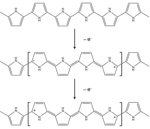
Many conformational and structural defects can be formed during polymerization process. Conformational defects are α-α bondings with nonregular rotation and structural defects involve α-β bonds, hydroxyl groups, and carbonyl groups, where α-β coupling leads to branching and crosslinking and the oxygen-containing groups are introduced by the oxidations, as illustrated in Figure 3. These defects introduce structural disorders in the polymer chain, affecting the conjugation length and electrical conductivity [17,18]
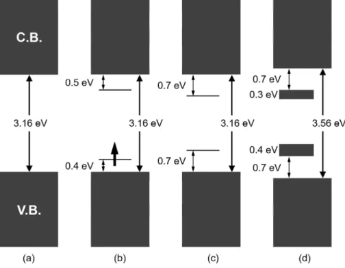
Figure 4 describes the four different electronic band structures by the transition for doping level of the PPY chain. In the neutral state, PPY is an insulator with a large π-π* band gap of ca. 3.16 eV.
However, when the PPY chain is doped with counterions to maintain electroneutrality during polymerization, a negative charge is extracted from the neutral segment of the chains. This gives rise to a local deformation from benzenoid to quinoid structure, forming a polaron.
proceeds further, another electron is removed from the chain, resulting in the formation of a double-charged bipolaron. At higher oxidation level (exceeding ca. 33 %), the overlap between bipolarons is occurred, resulting in the formation of two narrow bipolaronic bands.
This induces gradual diminution of band gap in terms of doping level, and Figure 5 portrays resulting alteration of PPY in chemical structures.
PPY can be readily prepared by electrochemical and chemical approaches in both aqueous and non-aqueous solutions, as mentioned previously. Electrochemical preparation of PPY is not very intriguing for commercialization because of the difficulties in mass production and higher price compared to chemical preparation. It was deeply studied that PPY-halogen complexes prepared by chemical oxidative polymerization reveal relatively high stability at ambient temperature.
Figure 3. Possible chemical structures in polypyrrole chains.
Figure 4. Electronic energy diagrams for (a) neutral, (b) polaron, (c) bipolaron, and (d) fully doped PPY.
Figure 5. Chemical structures of (a) neutral, (b) polaron in partially doped, and (c) bipolaron in fully doped polypyrrole.
1.1.2. Two-dimensional nanomaterials
Among a great number of nanomaterials, two-dimensional (2D) nanomaterials are generally categorized either 2D allotropes of various elements or compounds (Figure 6) [19–21]. 2D nanomaterials have attracted substantial attention from researchers since Novoselov, Geim, and co-workers discovered graphene after exfoliation from graphite using mechanical cleavage method in 2004. Considered the thinnest materials, these are either single layers, or comprise of several layers with strong in-plane bonding and sheet-to-sheet van der Waals interactions. The electron confinement in two dimensions of 2D nanomaterials enables tailorable electronic properties compared to other nanomaterials, making them appealing candidates for fundamental study of condensed matter as well as electronic device applications such as fabricating inks, pastes, catalysts, sensors, gene delivery, and energy harvesting devices [22–26].
Figure 6. Lattice structures and layer-dependent band structures of layered 2D nanomaterials [20].
1.1.2.1. MoS2nanosheet
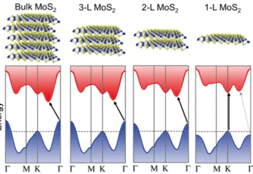
Molybdenum disulfide (MoS2) is one of transition-metal dichalcogenides (TMDCs), and an analogous layered structure with graphene consisting of a Mo atomic layer sandwiched by two S atoms layers as illustrated in Figure 7. MoS2 excels as a lubricant due to its layered structure as well as low coefficient of friction, dissipating energy by interlayer sliding when a shear stress is applied [27].
MoS2 nanosheets have received great attention because of their distinctive features such as size-tunable catalytic, electronic, and optical properties. The presence of unsaturated d-orbitals as well as chemically active edge sites leads to be an attractive candidate for many potential applications such as catalysts, transistors, and electrode materials for energy-storage systems. Silimarly to other layered nanomaterials, MoS2 exhibit band gap that can be differed from those in bulk [26–28]. As in Figure 8, the band gap changes from an indirect gap of 1.29 eV into a direct gap of 1.80 eV. In addition, MoS2 with odd number of layers could produce oscillating piezoelectric outputs. Therefore, unique characteristics of MoS2, e.g., size-dependent band gap tuning and unique 2D geometry, high electrochemical activity, and chemical stability make it utilized in
catalyst for hydrogen evolution, microelectronics, or photodetectors.
MoS2 nanosheet has attracted attention as a supercapacitor electrode material, still its low electrical conductivity limits its practical electrochemical performances despite a large number of advantages.
Especially by hybridization with conductive carbon materials or phase transition to metallic phase, MoS2 nanosheets can improve the electrochemical energy storage without the common restacking issues.
Liquid-phase exfoliation of 2D layered materials has become a widely used method to produce large quantity of 2D sheets from their parent bulk materials. 2D layered materials are constructed from a stacking of individual monolayers. Therefore, liquid-phase exfoliation requires the input energy enough to overcome the interlayer interactions. Accordingly, chemical or sonochemical exfoliation techniques of MoS2 have been developed to produce the 2D nanosheets [29-31]. This process has developed to indulge the demand of nanosheet inks for printed electronic devices [32,33].
Figure 7. Crystal structure of MoS2. (a) Top view of single layer hexagonal structure of MoS2. (b) Trigonal prismatic (2H) and octahedral (1T) unit cell structures [27].
Figure 8. Thickness-dependent band gap of MoS2 sheets. Bulk MoS2
shows an indirect band gap of 1.29 eV, whereas in its monolayer form it has a direct band gap of 1.80 eV [28].
1.1.2.2. Phosphorene
Black phosphorus (BP), a layered three-dimensional crystal consisted of a stack of puckered layers of P atoms, as displayed in Figure 9 [34]. BP has emerged as a next 2D nanomaterials recently, due to its exceptional characteristics. Among its characteristics, like other 2D nanomaterials, bulk BP has a direct band gap, and it changes its band gap depending on the number of layers, from 0.3 eV at bulk to 2.0 eV at single layer, as depicted in Figure 10 [35,36]. Hence, BP has great potential applications such as light-emitting diodes, transistors, photodetectors, and photovoltaics.
Nevertheless, BP still has hindrance to be commercialized since the conditions to synthesize BP are very demanding. For example, red phosphorus (RP) is one of the phosphorus allotropes, and can be converted to BP at 8.5 GPa [37]. BP also can be prepared by vapor transport method using RP and SnI2 at 500 ℃. Among the fabrication techniques, Figure 11 displays high-energy ball milling technique that induces the temperature enough for phase transition of RP to BP.
Accordingly, mechanical milling is a fascinating method to manufacture BP from RP in terms of mass production as well as cost savings [38,39].
The exfoliation energy of BP is found to be significantly greater than that of graphite, which accounts for the relative difficulty in exfoliating BP. Microcleavage of bulk BP using mechanical exfoliation (“scotch- tape” method), like the exfoliation of the graphene and TMDCs, can only produce small-size crystals. On the other hand, liquid-phase exfoliation (LPE), consisting of ultrasonic exfoliations of BP immersed into a solvent as shown in Figure 12, is suitable for large-scale production with a proper choice of solvent [40–43]. Furthermore, LPE can suppress the degradation of basal plane of phosphorene by choosing proper solvent like dimethylformaide (DMF), dimethyl sulfoxide (DMSO), and N-methyl-2-pyrrolidone (NMP). Still, its functionalization is necessary to utilize phosphorene as a building block of hybrid nanomaterials.
Figure 9. Schematic lattice structure of bulk BP, where P atoms at different sublayers are represented by different colors in each layer. (a) Top view of BP with AB stacking, and (b, c) side view of a single layer and N-layer BP, respectively [34].
Figure 10. Calculated electronic band structure of monolayer, bilayer, trilayer, and bulk BP sheets at all high-symmetery points in the Brillouin zone [36].
Figure 11. Schematic view of the motion of the ball and powder mixture [38].
Figure 12. Liquid-phase exfoliation of BP in various solvents via tip sonication. (a) Schematic and (b) photograph of the setup to minimize air exposure during exfoliation. (c) Photograph of a BP dispersion in NMP after ultrasonication and centrifugations. (d, e) BP concentration plot for various solvents depending on the boiling point and surface tension, respectively [40].
1.1.2.3. Graphene
Graphene is a single atomic layer of sp2 carbon atoms with a hexagonal honeycomb lattice as described in Figure 13 [44]. As mentioned above, first discovery of few- and single-layer graphene nanosheets by mechanical exfoliation by bulk graphite powders began to draw attention to many researchers. Namely, graphene comprises of tightly packed carbon atoms with sp2orbital hybridization, and it has a theoretical specific surface area of 2630 m2g–1, a remarkable electron mobility of 15000 cm2 V–1 s–1 at room temperature. A variety of exceptional properties such as unexpectedly high opacity and thermal conductivity, and the highest value of mechanical strength have led many to focus on graphene [45,46].
Figure 14 represents chemical vapor deposition (CVD), that it is one of the various methods that have been developed to produce large- scale graphene required for electronic device applications [47]. The large-scale production of graphene relies significantly on catalytic CVD. Ni and Cu (Figure 14a and b) are the most widely used catalysts due to their low cost, etchability and large grain size. In the case of Cu catalyst, the carbon intermediate is not dissolved in the Cu metal since the carbon solubility in Cu is negligible even at a very
high temperature, thus surface adsorption of carbon precursors formulates graphene. Usage of Cu catalyst for CVD-grown graphene is suggested to be self-liniting that once the single layer of graphene is grown, the process does not propagate anymore because of the blockage of Cu surface. The CVD-grown graphene, as a result, shows off aforementioned properties.
Figure 13. (a) Hexagonal honeycomb lattice of graphene with two atoms (A and B) per unit cell. (b, c) The 3D band structure and dispersion of the states of graphene. (d) Approximation of the low energy band structure as two cones contacting at the Dirac point [44].
Figure 14. Schematic diagrams of the possible distribution of C isotopes in the graphene films based on growth mechanisms of (a) segregation and/or precipitation growth and (b) surface adsorption [47].
1.1.3. Hybrid nanomaterials
The demand for hybrid nanomaterials is exploding as they are considered potential platforms for applications in incredibly diverse fields e.g. micro-electronics, transportations, energy storage, diagnosis, housing, optics, environment, and Internet of Things (IoT) [48–50].
The combination of inorganic materials with polymeric compounds provides an excellent functionality with high performance as well as enhanced stability and good processibility. However, many of the well-established materials have their own limits to fulfill all technological desires in various applications. Recent approaches on the design of functional hybrid materials have been conducted a lot, still the expectations go beyond the properties of the estabilished materials. Therefore, many efforts have been devoted to synthesize novel functionalized hybrid nanomaterials for their specified potential applications.
1.1.3.1. Integrative chemistry
There are numerous bottom-up strategies for the fabrication of functional hybrid materials (Figure 15) [51–53]. One strategy to fabricate hybrid nanomaterials is based on the assembly of preformed monodispersed nano-objects. The objects can be preformed before the assembly, such as surface functionalization with ligands, spacers, organic molecules, etc. The prefabrication of the monodispersed components can be utilized as building blocks for hybrid materials.
The nano-objects must be stable under the chemical conditions imposed during assembly. Accordingly, the components of the hybrid materials are linked by chemical bonds, allowing the development of well-defined structures that facilitate the performance of the final products [54,55].
Figure 15. Schematic representation of bottom-up approaches to nanocomposites: (a) nanomaterials are decorated by a second material without altering their morphology; (b) nanomaterials are partially consumed by a chemical reaction, leading ultimately to the desired composite material, and (c) preformed nanomaterials are controllably aseembled like Lego building blocks [53].
1.1.3.2 Vapor deposition polymerization
Vapor deposition polyqmerization (VDP) has become the subject of attention across a variety of fields, from electronic parts to biocompatible materials [56,57]. Especially, a facile fabrication of hybrid nanomaterials by coating of polymers with various substrates is available through one-step VDP, as described in Figure 16. The VDP proceeds in a sequence of liquid monomer injection, decompression, and polymerization of monomer vapors. The resultant polymer layer can be uniformly coated onto the surface of the hard template materials.
Figure 16. Schematic representation of the VDP for the encapsulation of the substrate materials [57].
1.1.4. Supercapacitor
Systems for electrochemical energy storage and conversion include batteries, fuel cells, and electrochemical capacitors [58]. These three systems have a common electrochemical base, although the storage and conversion mechanisms are different. Common features are that the energy-providing processes take place at the electrode/electrolyte interface and that electron and ion transport are separated. To compare the power and energy capabilities, a representative Ragone plot (Figure 17) discloses the relative positions of the energy-storing devices.
Among the so-called energy-storage system (ESS), electrochemical capacitor, or supercapacitor is used to describe a device that store an energy in the electrical double layer (EDL). As depicted in Figure 18, this EDL forms at the electrode/electrolyte interface with one layer at the surface inside the conductor and the other in the electrolyte almost instantaneously. When the charges are concentrated on each side of the electrode, the smaller ions are adsorbed, and the inner Helmholtz
Helmholtz plane (OHP), and these adsorption processes are determined by chemical affinities of the ions to the electrode and the field strength in the EDL. Unlike in batteries and fuel cells, the double layer at the electrode surface responds rapidly and the potential changes at the same time. When the physisorption/desorption process is only occurred, the device is called electric double-layer capacitor or electrostatic double-layer capacitor (EDLC). When the energy is mainly stored by a reversible faradaic charge transfer between electrolyte and electrode (pseudocapacitance), this type of capacitor is called pseudocapacitor [59].
Meanwhile, the innovative changes in the research and development of the electrochemical energy-storage devices lead to the proposal of several hybrid devices to satisfy the commercial views that have been formed on global warming and consumption of fossil fuels. Supercapattery, whose behavior is similar to that of supercapacitor with a greater energy capacity, is one of the proposed hybrid devices [60].
Figure 17. A relational position of supercapacitor and supercapattery to various energy technologies in Ragone plot [60].
Figure 18. Schematic representation of (a) the EDL structure of the interface between an aqueous electrolyte and a porous electrode; (b) explanations of symbols in (a); (c) potential distribution in the electrolyte solution between the negative and positive electrodes in an electrolysis cell [59,60].
1.1.4.1. Flexible supercapacitor
Flexible energy-storage devices are attracting considerable attention due to the rapidly growing demand in portable, flexible, and wearable electronic devices [61]. Particularly, flexible supercapacitors require the electrode materials with additional characteristics like well- integrated mechanical flexibility. Thus, typical flexible supercapacitors are based on highly flexible thin-film electrodes with soft materials as substates.
Carbon-based materials such as graphene, carbon nanotube, and carbon cloth are strong candidates among the available materials, possessing the sufficient mechanical strength to endure various mechanical stresses and excellent electrical conductivity. Pure carbon materials have a low packing density, thus the capacitance of these carbonaceous materials is limited. Therefore, the introduction of conducting polymers or transition metal oxides/hydroxides with pseudocapacitance has been regarded as a solution to further strengthen the electrochemical performance. By creating a hybrid
1.2. Objectives and Outlines 1.2.1. Objectives
In the precedent section, the significance of PPY-based 2D hybrid nanomaterials was introduced from the perspective on the practicability as well as academic research. The aim of this dissertation is to certify the fabrication method of PPY-based 2D hybrid nanomaterials with the prepared various 2D nanomaterials and to scrunitize their potentiality of supercapacitor. Particularly, 2D nanomaterials are fabricated by sonochemical exfoliation, phase transition and subsequent delamination, or CVD process, respectively.
Hybridization with PPY is proceeded according to the fabrication method either utilizing molecular bricks to build the intended hybrid material, called “integrative chemistry”, or VDP method. Moreover, the electrochemical behaviors and supercapacitor performance of the PPY/2D hybrid nanomaterials are systemically investigated to identify the optimal conditions for the efficient supercapacitor electrode.
1.2.2. Outlines
This doctoral dissertation involves the following subtopics:
I. Fabrication of few-layer MoS2 nanosheets and MoS2/PPY hybrid nanocomposites by non-covalent bonding
II. Fabrication of functionalized phosphorene and FP/PPY hybrid nanocomposites by covalent bonding
III. CVD-grown graphene/PPY nanocomposites by introduction of interfacial layer
Each subtopics contains experimental details, characterizations of fabricated materials, electrochemical behaviors and supercapacitor performances.
2. Experimental Details
2.1. Few-layer MoS2 nanosheets/PPY nanomaterials by non- covalent bonding
2.1.1. Materials
Molybdenum (IV) disulfide (MoS2, powder, < 2 μm, 99 %), pyrrole (98%), and FeCl3 (97%) were purchased from Aldrich Chemical Company and used without any purification. N-Methylpyrrolidone (NMP, 99.5%) and ethyl alcohol (99.5%) were purchased from Samchun chemicals.
2.1.2. Fabrication of few-layer MoS2nanosheets
Delamination of MoS2nanosheets from bulk MoS2 was carried out by grinding and sonochemical exfoliation. Bulk MoS2powders (4.0 g,
< 2 μm) were ground vigorously with NMP (4 mL) in a porcelain mortar for 30 min. Then, to remove all of the solvents, the mixture was placed in a vacuum oven. The dried powders were dispersed in a ethyl alcohol aqueous solution (45 vol%) by sonication for 2 h. After selecting the supernatants from the dispersion by leave the dispersion for 24 h, the dispersion was centrifuged to collect the MoS2nanosheet
powders to utilize them for the fabrication of MoS2/PPY hybrid nanomaterials.
2.1.3. Fabrication of few-layer MoS2/PPY (MPY) hybrid nano- materials
Few-layer MPY hybrid nanomaterials were prepared as follows.
Pyrrole monomer was diluted ten-fold in DI water. As-prepared MoS2
powders were put into a diluted aqueous solution of pyrrole monomer, which was then stirred for 2 h at the rate of 400 rpm. Pyrrole monomer was diluted in advance to improve the charge-charge interactions between MoS2 and pyrrole molecules. The reaction was conducted at different temperature. A micropipette was used to add FeCl3 aqueous solution (1 M), whose molar ratio of FeCl3 to pyrrole was fixed as 1.75:1, and the resulting solution was mixed at 6000 rpm for 30 min. This solution was centrifuged at 10,000 rpm and 5 ℃ to remove the residual reagents from the resultants, and then repeated for three times with additional DI water. The final product was washed
2.1.4. Electrochemical measurement of MPY hybrid-based super- capacitor
To measure the electrochemical properties of the MoS2/PPY nanomaterials, the materials were first dispersed in DI water at a concentration of 0.5 mg mL–1by ultrasonication at 30% amplitude for 30 min. The prepared solution was drop-casted onto Au/PEN current collector. All the electrochemical measurements were conducted in H2SO4 aqueous solution (1 M) as an electrolyte. Three-electrode system was comprised of the prepared MoS2/PPY electrode as a working electrode, Ag/AgCl in NaCl solution (3 M) as a reference electrode, and Pt wire as a counter electrode. Cyclic voltammetry (CV) was measured at a different scan rate in the range of 2 to 100 mV s–1. Specific capacitance from the result of cyclic CV was calculated by following equation.
= = ∫ 2 C: specific capacitance
Q: charge in Coulombs V: potential window
∫ : integral of CV curve : mass of specimen
: scan rate
In the case of galvanostat, the measurement was carried out with changing its specific current. The calculation of the specific capacitance from the result of galvanostatic charge-discharge curves was conducted by following equation,
= = I: applied current
t: discharge time
where other parameters are the same as above. Electrochemical impedance spectroscopy was measured at potentiostatic condition whose voltage was fixed as 10 mV and the frequency in the range of 107to 10–2Hz.
2.1.5. Characterization
Field-emission scanning electron microscopy (FE-SEM) images were collected using JSM-6701F (JEOL Ltd., Japan) installed at Seoul
Interuniversity Research Facilities (NCIRF) at Seoul National University. Topography of atomic force microscopy (AFM) was observed by a Digital Instrument Nanoscope IIIA (Veeco Instruments, Town of Oyster Bay, NY) in tapping mode with silicon tips (a resonant frequency of 320 kHz). X-ray photoelectron spectroscopy (XPS) spectra were obtained using Sigma probe (ThermoVG).
Loresta-GP/MCP-T610 (Mitsubishi) was used to measure the electrical conductivity at ambient temperature by four-point probe method. Lambda 35 (PerkinElmer, Waltham, MA) UV-visible spectrometer was utilized to acquire the electronic behaviors of the materials. All the electrochemical characterizations were conducted by ZIVE SP2 electrochemical workstation (WonATech, South Korea).
2.2. Functionalized phosphorene/PPY nanomaterials by covalent bonding
2.2.1. Materials
Red phosphorus (RP, powder, > 98.0 %) was purchased from Yakuri Pure Chemicals and used without any purification. pyrrole (98%), pyrrole-3-carboxylic acid (≥ 96%), and FeCl3 (97%) were obtained from Aldrich Chemical Company. Ethyl alcohol (99.5%) was purchased from Samchun chemicals.
2.2.2. Fabrication of phosphorene from red phosphorus
RP was phase transition of RP into black phosphorus (BP) by mechanical milling. RP powder (6 g) was put into a zirconia bowl with zirconia balls whose diameters are 1, 2, and 5 mm. The ball mill was conducted at 550 rpm and paused for 10 min for every 2 h, and a total duration of ball mill varied from 6 to 36 h. After milling, ethyl alcohol (30 mL) was poured into the bowl and it was milled at 400 rpm for 30 min. A mahogany-colored slurry was collected by
dried in a convection oven at 60 for 2 h. As℃ -prepared BP powder was dispersed in ethyl alcohol solution (45 vol% in water) and sonicated for 2 h. The solvent was then removed by centrifugation and the phosphorene powder was collected by drying the precipitates at RT in a vacuum oven for overnight. Aqueous solutions for exfoliation of BP can also be used, but with the addition of stabilizing surfactants together with deoxygenated water to avoid exposure of phosphorene to oxidizing species, in general. This fabrication method is focused on the mass production of phosphorene, thus, a small portion of oxidized species is acceptable.
2.2.3. Functionalization of phosphorene
As-prepared phosphorene powder (0.6 g) and urea (1.2 g) was put into the zirconia bowls, and the ball mill was carried out at 600 rpm for 2 h. After ball mill, ethyl alcohol (30 mL) was again poured into the bowl, milling at 400 rpm for 30 min. The solvent was removed after centrifugation and the functionalized phosphorene (FP) was collected by drying in a vacuum oven for overnight. The FP has a low stability against humidity, thus the product was stored in a dessicator before usage.
2.2.4. Fabrication of functionalized phosphorene/PPY (FPPY) hybrid nanomaterials
The prepared FP powder was dispersed in DI water which a concentration of FP was 1.0 mg mL–1 by sonication for 1 h. Before fabricating the nanomaterials, pyrrole and pyrrole-3-carboxylic acid was mixed (molar ratio of 30:1) until pyrrole-3-carboxylic acid was dissolved thoroughly. This mixture was used as a monomer of carboxylated PPY. The mixture of monomer was put into the FP solution, stirring at RT for 2 h. An aqueous solution of FeCl3 (1 M) was added with a fixed value of molar ratio of FeCl3 to monomer of 1.75, and reacted for 1 h.
2.2.5. Electrochemical measurement of FPPY hybrid-based super- capacitor
The electrochemical properties of the FP/PPY nanomaterials were analyzed by both potentiostat and galvanostat. First, the materials were dispersed by tip-sonicator in DI water at a concentration of 0.5
electrode system was comprised of the prepared hybrid nanomaterial electrode as a working electrode, Ag/AgCl in NaCl solution (3 M) as a reference electrode, and Pt wire as a counter electrode. Galvanostat as well as potentiostat were measured at a same condition of previous part mentioned before.
2.2.6. Characterization
Transmission electron microscopy (TEM) images and Raman spectra were obtained using a JEM-2100 (JEOL Ltd., Tokyo, Japan) and Horiba Scientific T64000 spectrometer at the National Center for Interuniversity Research Facilities (NCIRF) at Seoul National University, respectively. FT-IR spectra were collected with Frontier spectrophotometer (PerkinElmer). X-ray photoelectron spectroscopy (XPS) spectra were recorded using Sigma probe (ThermoVG). ZIVE SP2 electrochemical workstation (WonATech, South Korea) was used for all the electrochemical characterizations.
2.3. CVD-grown graphene/PPY hybrid nanomaterials by introduction of interfacial layer
2.3.1. Materials
Pyrrole (98%), FeCl3(97%), CuCl2(97%), dopamine hydrochloride (95%), and poly(vinyl alcohol) (PVA, average Mw 31,000–50,000) were purchased from Sigma-Aldrich Chemicals Company and used without any purification.
2.3.2. Chemical vapor deposition of graphene
Graphene was synthesized on polycrystalline copper foil by chemical vapor deposition (CVD) process. The copper foil was cut (8 cm × 8 cm) and was placed in the quartz-tube furnace. The temperature was increased to 1000 ℃ with a flow of H2 (8 sccm) under 140 mTorr of pressure, and held for 30 min. CH4 was introduced (20 sccm) for 20 min, and the furnace was cooled to room temperature. After the growth of the graphene, the other side of Cu foil was etched by atmospheric O plasma to remove excess graphene.
2.3.3. Fabrication of CVD-grown graphene/PPY (CDPY) hybrid nanomaterials by vapor deposition polymerization
Since the CVD-grown graphene barely has hydrophilic groups on the surface, the graphene was treated with atmospheric O2 plasma before applying dopamine solutions. Then, the dopamine solution and one of the initiator solutions, either FeCl3 (ferric chloride) or CuCl2
(cupric chloride), fully covered the graphene after spin coating in sequence. Both the dopamine and the initiator salts are dissolved in DI water in advance. Although the concentration of the dopamine varies in the range of 0.2–2.0 mg mL–1, that of the initiator solution is fixed as 1 M. In sequence, the film was placed into the glass apparatus to proceed vapor deposition polymerization. The gaseous pyrrole monomers were polymerized with previously applied initiators on the graphene, forming PPY layer under vacuum at RT, and the fabrication of either CDPY-Fe or CDPY-Cu, depending on the initiator, is completed. In the case of CPY-Fe or CPY-Cu, all the steps were conducted except for applying dopamine onto the CVD-grown graphene.
2.3.4. Electrochemical measurement of CDPY hybrid-based supercapacitor
High-resolution transmission electron microscopy (HR-TEM) and transmission electron microscopy (TEM) images were obtained using
A fabrication of all-solid-state full cell devices is conducted as follows. First, PVA powder was dissolved in the DI water (5 wt%) at 60 ℃, and the PVA solution was casted onto the quartz plate. The plate was heated at 60 ℃ for overnight to remove all of the solvent.
The PVA film was easily detached from the quartz plate, and the film was soaked completely in the H2SO4 aqueous solution (1 M). The residual solution on the film was wiped, and the prepared PVA/H2SO4
solid electrolyte film was sandwiched by two equivalent electrodes of CDPY-Fe nanomaterial. The stack was slightly pressed during the electrochemical measurements.
2.3.5. Characterization
A JEOL 6700 instrument was used to obtain FE-SEM images. The
Raman spectroscopy was conducted by Horiba Scientific T64000 spectrometer at the National Center for Interuniversity Research Facilities (NCIRF) at Seoul National University. ZIVE SP2 electrochemical workstation (WonATech) was used for all the electrochemical measurement, including potentiostat, galvanostat, and impedance spectroscopy.
3. Results and Discussion
3.1. MPY hybrid nanomaterials by non-covalent bonding 3.1.1. Fabrication of few-layer MoS2nanosheets
Bulk MoS2 powders are successfully exfoliated into few-layer MoS2 nanosheets. New additional steps for selecting a certain size of MoS2 nanosheets were carried out by centrifugation to acquire few- layer nanosheets, followed by precipitation and drying process to obtain MoS2 nanosheets in a powder form. The additional steps resulted in size selection of the few-layer nanosheets as well as a high- yield production which is imperative for commercialization. The final yield of few-layer MoS2nanosheets was approximately 62.5% [65].
The size and the morphology of the as-prepared few-layer MoS2
nanosheets were identified by TEM images in Figure 19a. It was confirmed the exfoliation of MoS2 whose lateral size was in the range of 200–400 nm. The bulk MoS2 powder was much larger, on the contrary, which the lateral size before the exfoliation was bigger than
ca. 5.1 nm, representing that the exfoliated MoS2 nanosheets consist of about five layers since the thickness of monolayer MoS2is close to 1 nm [66]
Raman spectroscopy was scrutinized to achieve structural understanding of the prepared few-layer MoS2nanosheets (Figure 20).
Two prominent peaks at 380 and 406 cm−1corresponds to the in-plane phonon mode E and out-of-plane phonon mode A of MoS2
nanosheets, respectively. Since the gap between two peaks becomes broader with more layers because of the stiffening of A peak, the number of the layer can be determined from its gap. Given that the gap between E and A was ca.25.7 cm−1, it can be estimated that the MoS2 nanosheets are comprised of five layers, in accordance with the thickness measured by AFM [65,67].
UV−Vis spectroscopy was investigated at room temperature to understand the electronic behaviors of the prepared few-layer MoS2
nanosheets (Figure 21). The resultant UV−vis spectrum provided information on the excitonic transitions in the MoS2nanosheets. Prior to measuring UV−vis spectroscopy, the MoS2 nanosheets were suspended and diluted in a mixture of ethyl alcohol and DI water.
Notable peaks were observed at 629 nm (1.97 eV) and 696 nm (1.78
eV), which suggest the existence of monolayer MoS2nanosheets. Two peaks verifies the direct transitions of A and B excitons at the K point of the Brillouin zone, respectively. Moreover, the shoulder peaks at 806 nm (1.54 eV) and 895 nm (1.39 eV) with small intensity correspond to the indirect-gap transitions of MoS2 nanosheets. These results were in reasonable agreement with previous results [68,69].
Figure 19. Topological analysis of the MoS2 nanosheets. (a) TEM image shows the lateral size of the MoS2 in the range of 200–400 nm, and (b) The average thickness by AFM is about 5.1 nm with small portion of unexfoliated flakes.
Figure 20. Raman spectrum of the MoS2nanosheets.
Figure 21. UV-visible spectrum of the MoS2nanosheets.
3.1.2. Fabrication of MPY nanomaterials
The MoS2 nanosheets who work as 2D inorganic substrate of PPY, were dispersed and stirred with different ratio of pyrrole to MoS2. A positive charge of pyrrole and a negative charge of MoS2 cause them being held together by non-covalent bonding. FeCl3 acts as an oxidizing agent for the polymerization of pyrrole, hence aqueous solution of FeCl3 (1 M) was added. A molar ratio of FeCl3 to pyrrole was fixed as 1.75:1 to maximize the electrical conductivity of PPY.
The reaction was initiated as soon as the addition of FeCl3 solution, changing its color to dark green.
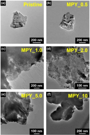
TEM images in Figure 22 are for the MoS2/PPY (MPY) hybrid nanomaterials, representing their morphological changes as a function of the gravimetric ratio of pyrrole to MoS2. The size, population and the morphology of decorated PPY is controlled. The materials of the hybrid MoS2/PPY with their ratios of pyrrole to MoS2are 0.5, 1.0, 2.0, 5.0, and 10 are denoted as MPY_0.5, MPY_1.0, MPY_2.0, MPY_5.0, and MPY_10, respectively. As in the TEM images, the formation of
to the transition of its morphology, MPY_2.0 has PPY nanospheres grown on the surface of MoS2with their radii ca.20 nm, respectively.
Furthermore, PPY begins to change its morphology from sphere to rod for MPY_5.0. A higher ratio of pyrrole makes PPY accretes with MoS2nanosheets with higher aspect ratio of ca.3.0. The morphology displays its transition again for MPY_10 that wad-like structure of PPY is formed.
Figure 22.TEM images of the (a) MoS2nanosheet and (b–e) the MPY
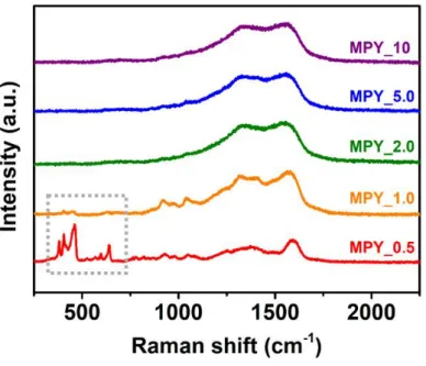
3.1.3. Material characterization of MPY hybrid nanomaterials The structural information about the MoS2/PPY hybrid nanomaterials was scrutinized by Raman spectroscopy using an excitation wavelength of 633 nm. All the samples were pelletized at a pressure of 7 metric ton for standardization. Figure 23 indicates Raman spectra of the MPY hybrid nanomaterials as a function of the gravimetric ratio between pyrrole and MoS2. Along with the TEM images representing PPY-decorated MoS2, the characteristic peaks from MoS2 as well as PPY were detected at the same time. To begin with, the PPY layer induced several peaks by its own bipolaron and polaron structures. The ring deformations attributed to bipolaron and polaron induced the peaks at 935, 984 cm–1, respectively. The peaks at 1056, 1083 cm–1are turned out to be C–H in-plane bending vibrations of reduction/oxidation states, respectively. The shoulder peak at 1257 cm–1 is from N–H in-plane deformation, and the peaks at 1369, 1414 cm–1 arise from C=C/C=N in-plane vibrations. In addition, C=C backbone stretching of reduction/oxidation states brought about the peaks at 1583, 1601 cm–1, respectively [70].
Besides, the characteristic peaks of MoS2 were observed simultaneously in the case of MPY_0.5 and MPY_1.0. Four major
peaks correspond to in-plane phonon E2g, out-of-plane phonon A1g, an overtone of longitudinal acoustic phonons at the M point of the Brillouin zone (2LA(M)), and an asymmetric translations of both Mo and S atoms along c-axis noticed at 381, 405, 452, and 462 cm–1[71].
The characteristic peaks of MoS2nanosheets were unnoticeable when the ratio of MoS2 was lower, and this is due to a low population of PPY in the hybrid nanomaterials. In other words, when PY/MoS2 of pyrrole to MoS2 is 2.0 or greater, PPY not only grows on the surface of the MoS2 nanosheets, but it fully covers the nanosheets, changing its morphology from nanosphere to nanorod to wad-like shape, as represented in TEM images.
X-ray photoelectron spectroscopy (XPS) was adopted to measure elemental composition and electronic state of the elements within the nanomaterials. Figure 24 displays the XPS spectra of MoS2/PPY nanomaterials that a deconvolution of the XPS spectra determines the fabrication of the materials. Three components are detected in C 1s region, which are C–C/C=C (284.5 eV), C–N (286.4 eV) bonds from
and are attributed to imine (–N=) group, amine (–NH–) group, positively charged nitrogen polaron (–NH+–) and bipolaron (=NH+–) of PPY, respectively [72,73]. In addition, it clarifies that the MoS2
nanosheets are connected with PPY by Mo–N bonding (394.7 eV), being formed during the polymerization [74,75]. The presence of Mo–
N bonds indicates that PPY layers have been formed on the surface of the MoS2 nanosheets, and the interaction lowers its interfacial resistance between MoS2and PPY, which will be discussed below.
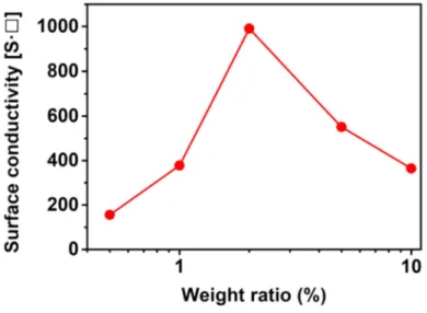
As one of the layered transition-metal dichalcogenides, MoS2 has poor electrical conductivity to be utilized as a supercapacitor electrode material, otherwise it limits its practicality of the electrochemical performance. Hence, a reinforcement of the electrical conductivity is necessary for MoS2 nanosheets. In especial, surface conductivity is one of the factors accurately affecting to supercapacitor performance.
Figure 25 represents the change of the surface conductivitiy of MPY hybrid nanomaterials as a function of the PY/MoS2 ratio. Pristine MoS2 nanosheet has its conductivity of 3.6 × 10⁻⁷ S sq., while the conductivity dramatically increases to 155 S sq. even when the PY/MoS2 weight ratio is 0.5 (MPY_0.5), the minimum. The surface conductivity keeps rising as more monomers take part in the reaction.
It shows an increment to 378, 991 S sq. in the case of MPY_1.0 and MPY_2.0, respectively. This change is resulting from the population growth of PPY layers on MoS2 nanosheets. The surface conductivity reveals its maximum value for MPY_2.0, which is due to population increment of the PPY nanospheres. As the PY/MoS2 ratio increases, the surface conductivity began to decrease that the MPY_5.0 and MPY_10. PPY nanospheres become agglomerated, and as a result, the conductivity of MPY hybrid was 552 and 364 S sq., respectively.
During the hybridization of PPY with MoS2 nanosheets, the large difference of the conductivity may induce the chain morphology more linearly [76]. The linearity was at its maximum when PY/MoS2is 2.0, and the α-β couplings began to increase with higher PY/MoS2ratios.
Figure 23. Raman spectra of MPY hybrid nanomaterials as a function of the PY/MoS2ratio from 0.5 to 10.
Figure 25. The change of surface conductivity of MPY hybrid nanomaterials as a function of the PY/MoS2ratio.
3.1.4. Electrochemical analysis of MPY hybrid nanomaterial- based supercapacitor
Electrochemical performance of the MoS2/PPY nanomaterials was investigated by cyclic voltammetry (CV). Beforehand, the MoS2/PPY nanomaterials were dispersed in DI water at a concentration of 0.5 mg mL–1 by ultrasonic homogenizer with its amplitude of 30% for 30 min with an interval of 1 s for every sonication for 3 s. The dispersions were drop-casted onto the Au/PEN substrates and dried at 60 for at ℃ least 4 h in a convection oven. The CV curves were measured in the three-electrode system that the prepared electrodes were utilized as working electrodes, Ag/AgCl (in 3 M NaCl) as a reference electrode, Pt wire as a counter electrode, and H2SO4 aqueous solution (1 M) as an electrolyte.
To verify the electrochemical properties of the MoS2/PPY nanomaterials, the CV curves were compared in Figure 26a. The CV was scanned at a same scan rate of 2 mV s–1 in the potential range of 0–0.9 V. Two distinctive peaks were the anodic peaks observed at
![Figure 6. Lattice structures and layer-dependent band structures of layered 2D nanomaterials [20].](https://thumb-ap.123doks.com/thumbv2/123dokinfo/11710035.0/31.773.138.639.183.384/figure-lattice-structures-layer-dependent-structures-layered-nanomaterials.webp)
![Figure 11. Schematic view of the motion of the ball and powder mixture [38].](https://thumb-ap.123doks.com/thumbv2/123dokinfo/11710035.0/40.773.156.633.202.554/figure-11-schematic-view-motion-ball-powder-mixture.webp)
![Figure 16. Schematic representation of the VDP for the encapsulation of the substrate materials [57].](https://thumb-ap.123doks.com/thumbv2/123dokinfo/11710035.0/50.773.141.633.203.502/figure-16-schematic-representation-vdp-encapsulation-substrate-materials.webp)
![Figure 17. A relational position of supercapacitor and supercapattery to various energy technologies in Ragone plot [60].](https://thumb-ap.123doks.com/thumbv2/123dokinfo/11710035.0/53.773.212.549.209.557/figure-relational-position-supercapacitor-supercapattery-various-technologies-ragone.webp)