저작자표시-비영리-변경금지 2.0 대한민국 이용자는 아래의 조건을 따르는 경우에 한하여 자유롭게
l 이 저작물을 복제, 배포, 전송, 전시, 공연 및 방송할 수 있습니다. 다음과 같은 조건을 따라야 합니다:
l 귀하는, 이 저작물의 재이용이나 배포의 경우, 이 저작물에 적용된 이용허락조건 을 명확하게 나타내어야 합니다.
l 저작권자로부터 별도의 허가를 받으면 이러한 조건들은 적용되지 않습니다.
저작권법에 따른 이용자의 권리는 위의 내용에 의하여 영향을 받지 않습니다. 이것은 이용허락규약(Legal Code)을 이해하기 쉽게 요약한 것입니다.
Disclaimer
저작자표시. 귀하는 원저작자를 표시하여야 합니다.
비영리. 귀하는 이 저작물을 영리 목적으로 이용할 수 없습니다.
변경금지. 귀하는 이 저작물을 개작, 변형 또는 가공할 수 없습니다.
2018년 2월 석사학위 논문
Study on Improved Morphology of Photoactive Layer for High
Efficiency Perovskite Solar Cells
조 선 대 학 교 대 학 원
화 학 과
김 한 솔
[UCI]I804:24011-200000266528
Study on Improved Morphology of Photoactive Layer for High
Efficiency Perovskite Solar Cells
고효율 페로브스카이트 태양전지를 위한 광활성층 몰폴로지 향상에 관한 연구
2018년 2월 23일
조 선 대 학 교 대 학 원
화 학 과
김 한 솔
Study on Improved Morphology of Photoactive Layer for High
Efficiency Perovskite Solar Cells
지도교수 이 재 관
이 논문을 이학석사학위신청 논문으로 제출함.
2017년 10월
조 선 대 학 교 대 학 원
화 학 과
김 한 솔
김한솔의 석사학위논문을 인준함
위원장 조선대학교 교수 손 홍 래 (인)
위 원 조선대학교 교수 김 호 중 (인)
위 원 조선대학교 교수 이 재 관 (인)
2017년 11월
조선대학교 대학원
TABLE OF CONTENTS
List of scheme ··· Ⅱ List of tables ··· Ⅲ List of figures ··· Ⅳ Abstract ··· Ⅶ
Chapter 1. ··· 1
Study on Improved Morphology of Photoactive Layer for High Efficiency Perovskite Solar Cells A. Introduction ··· 2
B. Experimental methods ··· 5
1. Materials 2. Solar cell fabrication 3. Measurements and instruments C. Result and discussion ··· 7
D. Conclusion ··· 30
E. Reference ··· 31
List of publications ··· 34
LIST OF SCHEME
Scheme 1 Schematic descriptions for preparation of MAPbI3(CB) and MAPbI3 (CB/DIO) films fabricated by time interval solvent-dripping with and without DIO additive, respectively, and their PHJ PrSC device structures.
LIST OF TABLES
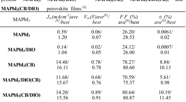
Table 1 Table 1. Photovoltaic performances of the p-i-n type PHJ PrSC devices with pristine MAPbI3, MAPbI3/DIO, MAPbI3(CB), MAPbI3/DIO(CB), and MAPbI3(CB/DIO) perovskite films.[a]
LIST OF FIGURES
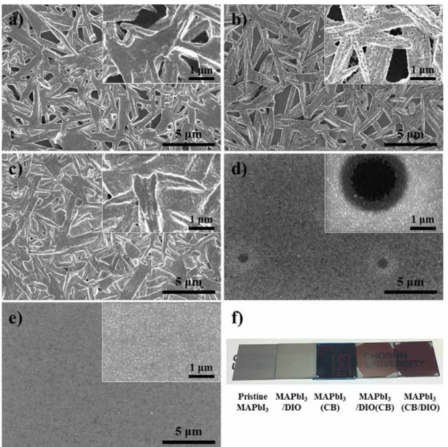
Figure 1 FESEM surface images of MAPbI3 perovskite films that were fabricated by varying casting method of MAPbI3 perovskite precursor in the DMF solvent on ITO/PEDOT:PSS substrates: (a) pristine MAPbI3, (b) MAPbI3/DIO, (c) MAPbI3(CB), (d) MAPbI3/DIO(CB), and (e) MAPbI3(CB/DIO) and (f) their picture images.
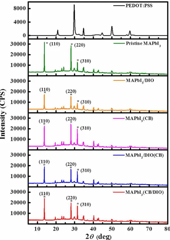
Figure 2 (a) XRD patterns of pristine MAPbI3 (green), MAPbI3/DIO (orange), MAPbI3(CB) (magenta), MAPbI3/DIO(CB) (blue), and MAPbI3(CB/DIO) (red) perovskite films.
Figure 3 J-V curves under AM 1.5 irradiation (100 mWcm-2) (a) average and (b) best performances obtained from the 44 individual p-i-n type
PHJ PrSC devices composed of
ITO/PEDOT:PSS/MAPbI3/PC61BM/Al fabricated with pristine MAPbI3 (green), MAPbI3/DIO (magenta), MAPbI3(CB) (black), MAPbI3/DIO(CB) (blue), and MAPbI3(CB/DIO) (red) perovskite films.
Figure 4 Distribution of photovoltaic performances for the 44 individual PHJ PrSC devices with MAPbI3(CB) (black), MAPbI3/DIO(CB) (blue), and MAPbI3(CB/DIO) (red) perovskite films.
Figure 5 (a) J-V curves for two individual PHJ PrSC devices fabricated with MAPbI3(CB) (black), MAPbI3/DIO(CB) (blue), and MAPbI3(CB/DIO) (red), perovskite films having large active areas of 14 mm2 on a substrate and (b) hysteretic J-V curve behavior under scanning in the forward and reverse directions for PHJ PrSC devices fabricated using MAPbI3(CB) (square) and MAPbI3(CB/DIO) (circle) perovskite film.
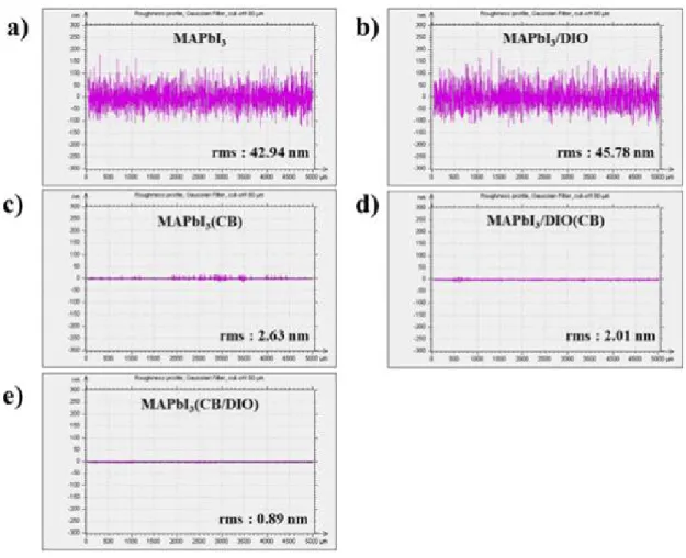
Figure S1 Surface roughness profiles of (a) pristine MAPbI3, (b) MAPbI3/DIO, (c) MAPbI3(CB), (d) MAPbI3/DIO(CB), and (e) MAPbI3(CB/DIO) perovskite films in 5 mm length scale.
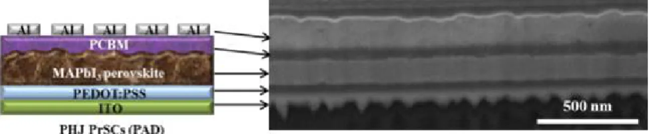
Figure S2 Cross-sectional FESEM image of PHJ PrSC device composed of ITO/PEDOT:PSS/MAPbI3/PC61BM/Alusedinthiswork.
Figure S3 Photovoltaic performances obtained from batch-to-batch on ten different dates for the 44 individual PHJ PrSC devices fabricated using MAPbI3(CB) perovskite films.
Figure S4 Photovoltaic performances obtained from batch-to-batch on ten different dates for the 44 individual PHJ PrSC device fabricated using MAPbI3/DIO(CB) perovskite films.
Figure S5 Photovoltaic performances obtained from batch-to-batch on ten different dates for the 44 individual PHJ PrSC device fabricated using MAPbI3(CB/DIO) perovskite films.
Figure S6 J-V curves for PHJ PrSC devices fabricated using MAPbI3(CB) and PC61BM processed with DIO(3vol%).
Figure S7 EQE spectra for PHJ PrSC devices fabricated using MAPbI3(CB) and PC61BM processed with DIO(3vol%).
Figure S8 FESEM surface images for grain size of MAPbI3 perovskite films that were fabricated by varying casting method of MAPbI3
perovskite precursor in the DMF solvent on ITO/PEDOT:PSS substrates: (a) pristine MAPbI3, (b) MAPbI3/DIO, (c) MAPbI3(CB), (d) MAPbI3/DIO(CB), and (e) MAPbI3(CB/DIO).
ABSTRACT
고효율 페로브스카이트 태양전지를 위한 광활성층 몰폴로지 향상에 관한 연구
Kim Hansol
Advisor : Prof. Lee Jae Kwan, Ph.D.
Department of Chemistry
Graduate School of Chosun University
A processing additive dripping (PAD) approach to forming highly efficient (CH3NH3)PbI3 (MAPbI3) perovskite layers was investigated.
고효율 (CH3NH3)PbI3 (MAPbI3) 페로브스카이트(perovskite) 층을 형성하기 위 한 processing additive dripping (PAD) 방법이 조사되었다.
A MAPbI3(CB/DIO) perovskite film fabricated by this approach, which included briefly dripping chlorobenzene incorporating a small amount of diiodooctane (DIO) during casting of a MAPbI3 perovskite precursor dissolved in dimethylformamide, exhibited superior smooth, uniform morphologies with high crystallinity and large grains and revealed completely homogeneous surface coverage.
Dimethylformamide에 용해된 MAPbI3 페로브스카이트 전구체를 주조하는 동안 소량의 diiodooctane (DIO)을 포함하는 클로로벤젠(CB)을 간단히 dripping하 는 방법으로 제조된 MAPbI3(CB/DIO) 페로브스카이트는 높은 결정성 및 넓은 표면을 완전히 균일하게 나타냈다.
The surface coverage and morphology of the substrate significantly affected the photovoltaic performance of planar heterojunction (PHJ) perovskite solar cells (PrSCs), resulting in a power conversion efficiency of 11.45% with high opencircuit voltage of 0.91 V and the highest fill factor of 80.87 %.
기판의 흡착률 및 몰폴로지는 평면 헤테로 접합(PHJ) 페로브스카이트 태양 전지(PrSCs)의 광전지 성능에 중대한 영향을 미쳤으며, 0.91V의 높은 개방회 로 전압(opencircuit voltage)과 80.87 %의 가장 높은 충전 계수(fill factor)로 11.45 %의 전력 변환 효율(power conversion efficiency)을 가져 온다.
Moreover, the PAD approach could effectively provide efficient MAPbI3(CB/DIO) perovskite layers for highly efficient, reproducible, uniform PHJ PrSC devices without performance loss or variation even over larger active areas.
더욱이, PAD 접근법은 보다 큰 활성 영역에 걸쳐서도 성능 손실이나 변동 없 이 높은 효율, 재현성, 균일한 PHJ PrSC 장치를 위한 효율적인 MAPbI3 (CB/DIO) 페로브스카이트 층을 효과적으로 제공 할 수 있다.
Keywords: organometal halide · perovskite solar cell · planarheterojunction · processing additive · solvent dripping
Chapter 1.
Study on Improved Morphology of Photoactive
Layer for High Efficiency Perovskite Solar Cells
A. Introduction
Organometal halide perovskite solar cells (PrSCs) have recently received considerable attention in the scientific community because they have exhibited breakthrough power conversion efficiencies (PCEs) of ~20 %, making them promising alternatives to conventional silicon-based solar cells.[1] The organometal halides, especially alkylammonium lead halides, (RNH3)PbX3 (R=alkyl, X=Cl, Br, I), are direct-band-gap materials with hybrid organic-inorganic perovskite structures; they exhibit outstanding performance as electron and hole conductors and also as photosensitizers.[2] Notably, both the electron and hole diffusion lengths were determined on long-ranged scales of ~100 nm and above 1 mm in triiodide (CH3NH3)PbI3 (MAPbI3) and mixed halide (CH3NH3)PbI3-xClx perovskite materials, respectively.[3] Most of the very high PCEs have been achieved in mesoscopic PrSCs, having an n-i-p type device architecture with a mesoscopic metal oxide layer such as TiO2 and require high temperatures of above 450℃ to build mesoporous structures in the metal oxide layer.[1b, 2c, 4] However, solution-processable organometal halide planar heterojunction (PHJ) PrSCs have been of great interest very recently because of their facile and inexpensive manufacturing processes, including versatile methods such as inkjet, doctor-blade, and roll-to-roll printing.[1i, 5] These p-i-n type PrSCs have often been fabricated using PHJ bilayer structures of perovskite materials and an electron-transporting material such as [6,6]-phenyl-C(61 or 71)-butyric acid methyl ester (PC(61 or
71)BM).[1j]
In particular, because the crystallinity, uniformity, and coverage of perovskite materials on the substrate are critical to improving the PCEs of devices, there has been extensive research on developing efficient methods for the fabrication of perovskite material layers in PHJ PrSCs. The following strategies have been adopted for this purpose: (1) interdiffusion by sequential spin-casting or simultaneous vacuum deposition of a metal halide such as PbI2 and an
alkylammonium halide such as CH3NH3I,[2b, c, 6] and (2) direct casting of a perovskite precursor solution with various types of thermal annealing,[7]
solvent-engineering,[4, 8] adduct,[9] processing additive treatment,[10] or components.[11] Among them, solvent-engineering in which a solvent such as toluene, chlorobenzene, or ether is dripped briefly during casting of he perovskite precursor significantly improved crystallinity, uniformity, and coverage of perovskite materials,[4, 7b, 12] Also, incorporating a small amount of a processing additive such as dihaloalkane, chloronaphthalene, or ammonium halide into the perovskite precursor solution induced high crystallinity and a better morphology.[10] These methods provided sufficiently high PCEs in PHJ PrSCs.
However, the PHJ PrSCs were often fabricated with a small active area and still suffer from a large variation in device performance because the perovskite crystal grains were randomly formed in the solution-processed films. Thus, it is challenging to find methods that enhance the uniformity of the film morphology toward large area PHJ PrSCs, which are essential for commercial application.
On the other hand, very recently, we reported improved efficiency in organic solar cells having a ternary bulk heterojunction (TBHJ) configuration consisting of nanostructured MAPbI3 perovskite-low bandgap polymer-PCBM.[13] The TBHJ device constructed with a PCPDTBT-PCBM bulk heterojunction (BHJ) integrated on diiodooctane (DIO)-treated MAPbI3 perovskite nanostructures exhibited better photovoltaic performance than a BHJ device without perovskite materials. DIO treatment of MAPbI3 nanostructures played a key role in developing perovskite crystallinity. In addition, the additive reportedly helped to form a smooth and uniform film with flawless perovskite nanocrystals.[10] Thus inspired, we attempted to induce a more uniform morphology in perovskite films by using the processing additive dripping (PAD) approach, in which a solvent incorporating a small amount of DIO processing additive is briefly dripped during casting of the perovskite precursor. We speculated that PHJ PrSCs with perovskite materials fabricated by the PAD method may exhibit superior performance with little
variation and be applicable to larger area devices.
Herein, we report improved efficiency in PHJ PrSCs with a MAPbI3(CB/DIO) perovskite film by a simple PAD approach, which was readily demonstrated by briefly dripping chlorobenzene incorporating a small amount of diiodooctane (DIO) during casting of a MAPbI3 perovskite precursor dissolved in dimethylformamide (DMF). These films, cast on an the indium tin oxide (ITO)/poly(3,4-ethylenedioxythiophene):poly-(styrenesulfonate)(PEDOT:PSS) substrate by the PAD method exhibited a superior smooth, uniform morphology with high crystallinity and large grain and were compared with pristine MAPbI3 and MAPbI3/DIO fabricated from precursor solution without and with DIO additive, respectively, and MAPbI3(CB) and MAPbI3/ DIO(CB) fabricated by briefly dripping chlorobenzene during casting of the precursor solution with and without DIO additive, respectively.
Notably, the p-i-n type PHJ PrSC device consisting of ITO/PEDOT:
PSS/MAPbI3(CB/DIO)/PC61BM/Al exhibited a improved efficiency compared those with pristine MAPbI3, MAPbI3/DIO, MAPbI3(CB), or MAPbI3/DIO(CB). Further, the results obtained using the PAD approach showed high batch-to-batch reproducibility and high uniformity, with little variation between individual devices on the substrate, which is suitable for large-area devices. Scheme 1 shows the preparation of MAPbI3(CB) and MAPbI3(CB/DIO) perovskite films fabricated by briefly dripping a solvent with or without DIO additive and their PHJ PrSC device architectures, in which there are five individual solar cell devices on a substrate.
B. Experimental Section 1. Materials
PbI2 was purchased from Aldrich and CH3NH3I was prepared according to a method reported previously.[1g] All solvents were purchased from Sigma–Aldrich, TCI, and Alfa Aesar and were purified using appropriate methods. The MAPbI3 precursor solution was prepared under a nitrogen atmosphere. The PCBM was obtained from Nano-C.
2. Solar cell fabrication
ITO-coated glass substrates were cleaned with detergent, ultrasonicated in acetone and isopropyl alcohol, and dried overnight in an oven. PEDOT:PSS (Heraeus, Clevios P VP.AI 4083) in an aqueous solution was spin-cast on the ITO substrates to form a film ~35 nm in thickness. The substrate was dried for 10 min at 140℃ in air and transferred into a glove box for spin-casting of the MAPbI3 precursor solution. The MAPbI3 precursor solution was prepared using PbI2 and CH3NH3I (molar ratio, 1:1) in DMF at 60 wt% and stirred at 60℃ for 12 h. MAPbI3 perovskite films were deposited on the PEDOT:PSS/ITO substrate a follows: (i) pristine MAPbI3: spin-casting at 5000 rpm for 30 s using the MAPbI3 precursor solution, (ii) MAPbI3/DIO: spin-casting at 5000 rpm for 30 s using the MAPbI3 precursor solution with DIO additive (3 vol %), (iii) MAPbI3(CB): spin-casting at 5000 rpm for 30 s using the MAPbI3 precursor solution followed by dripping of chlorobenzene in 6 s, (iv) MAPbI3/DIO(CB):
spin-casting at 5000 rpm for 30 s using the MAPbI3 precursor solution with DIO additive (3 vol%) followed by dripping of chlorobenzene in 6 s, (v) MAPbI3(CB/DIO) spin-casting at 5000 rpm for 30s using the MAPbI3 precursor solution with DIO additive (3 vol%) followed by dripping of chlorobenzene with DIO additive (3 vol%) in 6 s. Then, the substrate was dried on a hot plate at 100℃ for 10 min. The PC61BM solution were spin-cast on top of the MAPbI3
layer followed by heat-treatment at 80℃ for 10 min. Finally, an Al metal electrode of thickness ~100 nm was deposited on top of the MAPbI3/PC61BM PHJ film under reduced pressure (less than 10-6 Torr).
3. Measurements and instruments
The surface morphologies were imaged using a FESEM (NovananoSEM 450, FEI, Netherlands). The perovskite crystallinities of MAPbI3 films were investigated using XRD (D/Max2500 V/PC, Rigaku Corp, Japan). The solar cells efficiencies were characterized under simulated 100 mWcm-2 AM 1.5G irradiation from a Xe arc lamp with an AM 1.5 global filter. The simulator irradiance was characterized using a calibrated spectrometer and the illumination intensity was set using a silicon diode with an integrated KG1 optical filter certified by the National Renewable Energy Laboratory. The spectral mismatch factors were calculated to be less than 5% for each device. The short circuit currents were also found to be within 5% of the values calculated using the integrated external quantum efficiency spectra and the solar spectrum. The applied potential and cell currents were measured using a Keithley model 2400 digital source meter. The current-voltage (J-V) curves were measured at a voltage settling time of 100 ms.
The J-V curves were measured at a voltage settling time of 100 ms. The short circuit currents were also observed to be within 5% of the values calculated using the integrated external quantum efficiency (EQE) spectra and the solar spectrum. The applied potential and cell currents were measured using a Keithley 2400 digital source meter. The J-V curves were measured at a voltage settling time of 100 ms. The EQEs were measured by under filling the device area using a reflective microscope objective to focus the light output from a 75 W Xe lamp, a monochromator, and an optical chopper. The photocurrent was measured using a lock-in amplifier, the absolute photon flux was determined using a calibrated silicon photodiode and was recorded for 5 s per point (80 points) between 350–1100 nm.
C. Result and discussion
Figure 1 presents (a–e) field emission scanning electron microscope (FESEM) surface images and (f) photographs of MAPbI3 perovskite films fabricated by varying methods of casting a MAPbI3 perovskite precursor in DMF solvent on ITO/PEDOT:PSS substrates: (a) pristine MAPbI3, (b) MAPbI3/DIO, (c) MAPbI3(CB), (d) MAPbI3/DIO(CB), and (e) MAPbI3(CB/DIO). Figure 1a and 1b show the pristine MAPbI3 and MAPbI3/DIO films cast from the precursor solution without and with DIO additive, which generally exhibited longitudinal morphologies with sparse surface coverage on the ITO/PEDOT:PSS substrate. In addition, a rather large number of pinholes appeared sporadically in the MAPbI3/DIO perovskite morphology. They might be caused by the DIO additive in the MAPbI3 precursor solution. The pristine MAPbI3 and MAPbI3/DIO perovskite films exhibited poor transparency and high turbidity, as shown in Figure 1 f. Meanwhile, the MAPbI3(CB) perovskite film cast from the precursor solution with solvent dripping also exhibited not only longitudinal morphologies like those of MAPbI3 and MAPbI3/DIO, but also well-formed surface coverage on the ITO/PEDOT:PSS substrate, as shown in Figure 1c. Note that the solvent dripping during casting of the MAPbI3 precursor solution can obviously help to fill the gaps between the longitudinal features with sparse surface coverage on the ITO/PEDOT:PSS substrate. However, as shown in Figure 1d and 1e, there were no directional morphologies in the MAPbI3/DIO(CB) and MAPbI3(CB/DIO) perovskite films showed more smooth and uniform surface morphologies than MAPbI3(CB). The surface uniformity of the pristine MAPbI3, MAPbI3/DIO, MAPbI3(CB), MAPbI3/DIO(CB), and MAPbI3(CB/DIO) perovskite films could be also determined in length scale of 5 mm using the surface profiling analysis, showing in the root-mean-square roughness values of 42.94, 45.78, 2.63, 2.01, and 0.89 nm (see Figure S1 in the Supporting Information). These were closely correlated with their surface morphologies shown in Figure 1. Interestingly, the
MAPbI3(CB/DIO) perovskite film revealed completely homogeneous surface coverage on the ITO/PEDOT:PSS substrates, whereas many pinholes with large diameters of 1~3 mm appeared throughout the MAPbI3/DIO(CB) perovskite film.
These pinholes are thought to results from washing of DIO additive from the MAPbI3/DIO(CB) perovskite film during chlorobenzene dripping. The MAPbI3(CB), MAPbI3/DIO(CB), and MAPbI3(CB/DIO) perovskite films exhibited much better transparency than the MAPbI3 and MAPbI3/DIO perovskite films (Figure 1 f). These results indicate that the PAD method might be very useful and important approach with synergetic effects from DIO additive and solvent dripping to improve the performance of PHJ PrSCs. The surface coverage and morphology of the substrate might significantly affect the photovoltaic performance of the PHJ PrSCs, as discussed below.
Scheme 1. Schematic descriptions for preparation of MAPbI3(CB) and MAPbI3(CB/DIO) films fabricated by time interval solvent-dripping with and without DIO additive, respectively, and their PHJ PrSC device structures.
Figure 1. FESEM surface images of MAPbI3 perovskite films that were fabricated by varying casting method of MAPbI3 perovskite precursor in the DMF solvent on ITO/PEDOT:PSS substrates: (a) pristine MAPbI3, (b) MAPbI3/DIO, (c) MAPbI3(CB), (d) MAPbI3/DIO(CB), and (e) MAPbI3(CB/DIO) and (f) their picture images.
Figure S1. Surface roughness profiles of (a) pristine MAPbI3, (b) MAPbI3/DIO, (c) MAPbI3(CB), (d) MAPbI3/DIO(CB), and (e) MAPbI3(CB/DIO) perovskite films in 5 mm length scale.
Figure 2 shows the X-ray diffraction (XRD) patterns of the pristine MAPbI3, MAPbI3/DIO, MAPbI3(CB), MAPbI3/DIO(CB), and MAPbI3(CB/DIO) perovskite films. The XRD patterns exhibited the typical perovskite crystallinity of MAPbI3 without the typical patterns of PbI2.[2b] The (310) directional crystallinity of MAPbI3 perovskite was observed with much lower peak intensities in the XRD patterns of the pristine MAPbI3 and MAPbI3/DIO films than in those of MAPbI3(CB), MAPbI3/DIO(CB), and MAPbI3(CB/DIO). These results were in good agreement with the structural morphologies shown in Figure 1. Notably, the (110) peak in the XRD pattern of MAPbI3(CB) perovskite film exhibited a somewhat lower intensity than the (220) peak compared to those in other perovskite films, indicating that the solvent dripping approach might induce (220) and (310) directional crystal growth of MAPbI3 perovskite.
Figure 2. (a) XRD patterns of pristine MAPbI3 (green), MAPbI3/DIO (orange), MAPbI3(CB) (magenta), MAPbI3/DIO(CB) (blue), and MAPbI3(CB/DIO) (red) perovskite films.
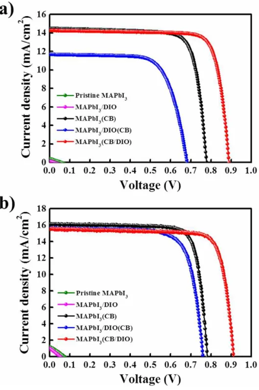
Next, PHJ PrSC devices were fabricated using the pristine MAPbI3, MAPbI3/DIO, MAPbI3(CB), MAPbI3/DIO(CB), and MAPbI3(CB/DIO) perovskite films and PC61BM. Figure 3 shows the current density-voltage (J-V) curves under AM 1.5 irradiation (100 mWcm-2), where panels (a) and (b) show the average and best performances, respectively of 44 individual p-i-n type PHJ PrSC devices composed of ITO/PEDOT:PSS/MAPbI3/PC61BM/Al fabricated using pristine MAPbI3, MAPbI3/DIO, MAPbI3(CB), MAPbI3/DIO(CB), and MAPbI3(CB/DIO) perovskite films. The corresponding values are summarized in Table 1. As shown in Figure 3 and Table 1, the PHJ PrSC devices fabricated using pristine MAPbI3 and MAPbI3/DIO perovskite films exhibited very poor photovoltaic performance.
This might be the results of their poor morphologies and sparse surface coverages (Figure 1). Meanwhile, most of the PHJ PrSC devices in which the films were fabricated using the solvent dripping approach with/without DIO additive showed significantly improved photovoltaic performance compared to those using pristine MAPbI3 and MAPbI3/DIO perovskite films because of the full coverage and good surface morphologies of the MAPbI3(CB), MAPbI3/DIO(CB), and MAPbI3(CB/DIO) perovskite films. The PHJ PrSC devices with MAPbI3(CB), MAPbI3/DIO(CB), and MAPbI3(CB/DIO) perovskite films exhibited a PCE (best/average) of 10.13 %/8.84% with a short-circuit current density (Jsc) (best/average) of 16.11/14.48 mAcm-2, an open-circuit voltage (Voc) (best/average) of 0.78/0.78 V, and fill factor (FF) (best/average) of 80.60 %/78.27 %; a PCE of 8.98 %/5.61% with Jsc=15.67/11.68 mAcm-2, Voc=0.76/0.68 V, and FF=75.37%/
70.59 %; and a PCE of 11.45/10.19% with Jsc=15.56/ 14.20 mAcm-2, Voc=0.91/0.89 V, and FF=80.87 %/80.64 %, respectively. Although these values, especially Jsc, were relatively low compared to those reported previously, this is attributed to the low thickness of the MAPbI3 used in this work (~250:30 nm) owing to the high spin-casting rate of 5000 rpm, despite the MAPbI3 precursor concentration of 60 wt% (Figure S2). As shown in Figure 3a, the best PCE of 11.45% was observed in the PHJ PrSC device with MAPbI3(CB/DIO) perovskite
Table 1. Photovoltaic performances of the p-i-n type PHJ PrSC devices with
pristine MAPbI3, MAPbI3/DIO, MAPbI3(CB), MAPbI3/DIO(CB), and MAPbI3(CB/DIO) perovskite films.[a]
MAPbI3 Jsc(mAcm-2)ave
[b]/best
Voc(V)ave[b]/ best
F.F (%) ave[b]/best
η (%) ave[b]/best
MAPbI3 0.39/
1.20
0.06/
0.07
26.20/
28.53
0.0061/
0.02
MAPbI3/DIO 0.14/
1.04
0.02/
0.05
24.12/
26.00
0.0007/
0.01
MAPbI3(CB) 14.48/
16.11
0.78/
0.78
78.27/
80.60
8.84/
10.13
MAPbI3/DIO(CB) 11.68/
15.67
0.68/
0.76
70.59/
75.37
5.61/
8.98
MAPbI3(CB/DIO) 14.20/
15.56
0.89/
0.91
80.64/
80.87
10.19/
11.45 [a] The performances are determined under simulated 100 mWcm-2 AM 1.5 illumination. The light intensity using calibrated standard silicon solar cells with a proactive window made from KG5 filter glass traced to the NREL. The active area of device is 4.5 mm2. [b] These values were determined from the average of individual 44 solar cells.
films; it showed a higher Voc of 0.91 V and F.F of 80.87 %, which might be the highest record FF value compared with those of p-i-n type PHJ PrSC devices composed of ITO/PEDOT: PSS/MAPbI3/PC61BM/Al reported previously,[14]
despite the slightly lower Jsc value than the device with MAPbI3(CB) and MAPbI3/DIO(CB) perovskite films. These improvements in Voc and FF might originate from the superior smooth morphology and surface coverage of the perovskite film, resulting in less recombination in interfaces with PEDOT:PSS (or PCBM).[15] Although these best PCE values in solar cell devices have been considered the most important achievement, we often find it difficult to reproduce the best performance.
Figure 3. J-V curves under AM 1.5 irradiation (100 mWcm-2) (a) average and (b) best performances obtained from the 44 individual p-i-n type PHJ PrSC devices composed of ITO/PEDOT:PSS/MAPbI3/PC61BM/Al fabricated with pristine MAPbI3 (green), MAPbI3/DIO (magenta), MAPbI3(CB) (black), MAPbI3/ DIO(CB) (blue), and MAPbI3(CB/DIO) (red) perovskite films.
Figure S2. Cross-sectional FESEM image of PHJ PrSC device composed of ITO/PEDOT:PSS/MAPbI3/PC61BM/Alusedinthiswork.
Thus, we obtained these J-V curves from the average performance of 44 individual PHJ PrSC devices fabricated under the same conditions on different dates, which might be important to demonstrate the batch-to-batch reproducibility of the device performance. As shown in Figure 3b and Table 1, the PHJ PrSC devices fabricated using MAPbI3(CB) and MAPbI3/DIO(CB) perovskite films exhibited average PCEs of 8.84% and 5.61 %, respectively, showing large variations in Jsc values with their best performances, whereas the PHJ PrSC devices fabricated with MAPbI3(CB/DIO) perovskite films exhibited an average PCE of 10.19 %, showing a rather small variation in all parameter values from its best performance compared those using MAPbI3(CB) and MAPbI3/DIO(CB) perovskite films. Also these device performances were compared from batch-tobatch on ten different dates (see Figure S3–S5 in Supporting Information).
These results might originate in smoother surface and more complete coverage of the MAPbI3(CB/DIO) perovskite film compared to the MAPbI3(CB) and MAPbI3/DIO(CB) perovskite films as shown in Figure 1.
Figure S3. Photovoltaic performances obtained from batch-to-batch on ten different dates for the 44 individual PHJ PrSC devices fabricated using MAPbI3(CB) perovskite films.
Figure S4. Photovoltaic performances obtained from batch-to-batch on ten different dates for the 44 individual PHJ PrSC device fabricated using MAPbI3/DIO(CB) perovskite films.
Figure S5. Photovoltaic performances obtained from batch-to-batch on ten different dates for the 44 individual PHJ PrSC device fabricated using MAPbI3(CB/DIO) perovskite films.
Figure 4 shows the distributions of the photovoltaic performance parameters of the 44 individual PHJ PrSC devices with MAPbI3(CB), MAPbI3/DIO(CB), and MAPbI3(CB/DIO) perovskite films. The PHJ PrSC devices fabricated using MAPbI3/DIO(CB) films exhibited irregular distributions with a large variation in all the parameters: PCEs=5.17 %–8.98 %, Jsc=8.00-15.67 mAcm-2, Voc=0.53–0.90 V, and FF=68.62 %–81.87 %. These might be the results of the nonuniform surface morphologies with large pinholes observed in the MAPbI3/DIO(CB) perovskite film. The PHJ PrSC devices fabricated using MAPbI3(CB) perovskite films exhibited a more regular distribution than those with MAPbI3/DIO(CB) perovskite films, but rather large variation in all the parameters, especially the Jsc values: PCEs=7.61–10.13%, Jsc=11.42–16.67 mAcm-2, Voc=0.71–0.83 V, and FF=67.58–81.30 %. Notably, the PHJ PrSC devices fabricated using MAPbI3(CB/DIO) perovskite films exhibited the most regular distribution with small variation and high performance in all the parameters: PCEs=9.0–11.45 %, Jsc=12.67–15.56 mAcm-2, Voc=0.85–0.94, and FF=78.48–81.94 %. These results indicate that the PAD approach can effectively provide superior surface morphologies in perovskite films for highly efficient and reproducible PHJ PrSC devices.
Figure 4. Distribution of photovoltaic performances for the 44 individual PHJ PrSC devices with MAPbI3(CB) (black), MAPbI3/DIO(CB) (blue), and MAPbI3( CB/DIO) (red) perovskite films.
On the other hand, PHJ PrSCs have often shown the best performance for device structures with a small active area, but still suffer from rather poor performance when the active area is large. We speculated that the high uniformity of a solutionprocessed perovskite film cast on a substrate might help to achieve high efficiencies on large-area PHJ PrSCs without performance loss or variation because the solution-processed PHJ PrSCs often have randomly formed perovskite crystal grains and surface morphologies. Figure 5 shows (a) the J-V curves of high efficiency PHJ PrSC devices fabricated using MAPbI3(CB), MAPbI3/DIO(CB), and MAPbI3(CB/DIO) perovskite films having three times larger active areas of 14 mm2 compared to those (4.5 mm2) shown in Figure 4 and (b) hysteretic J–V curve behavior under scanning in the forward and reverse directions for PHJ PrSC devices fabricated using MAPbI3(CB) and MAPbI3( CB/DIO) perovskite films. As shown Figure 5a, in this device architecture, there are two individual solar cell devices on a substrate. Two PHJ PrSC devices fabricated using MAPbI3/DIO(CB) perovskite films on a substrate presented a large variation in the Voc and FF values and two PHJ PrSC devices fabricated with MAPbI3(CB) perovskite films on a substrate exhibited a slight variation in the FF values, whereas two PHJ PrSC devices fabricated using MAPbI3(CB/DIO) perovskite films on a substrate exhibited almost the same photovoltaic performance, showing the comparable efficiencies with those with active area of 4.5 mm2 on a substrate. These results indicate that the high uniformity of MAPbI3(CB/DIO) perovskite films cast on a substrate could enable PHJ PrSCs to achieve high efficiencies without performance loss or variation between devices, even over a larger active area, compared to MAPbI3(CB) and MAPbI3/DIO(CB) perovskite films. Besides, we often find large hysteretic J-V curve behavior in PrSC devices under scanning in the forward and reverse directions, where the forward scan generally yields better performance than the reverse scan,[16]
However, the p-i-n type PHJ PrSC device configuration of ITO/PEDOT:PSS/MAPbI3/PC61BM/Al showed negligible hysteretic J-V curve behavior under forward and reverse scans.[17] The PHJ PrSC devices fabricated using MAPbI3(CB) perovskite films also exhibited a negligible hysteretic J-V curve. Interestingly, the PHJ PrSC devices fabricated using MAPbI3(CB/DIO) perovskite films exhibited better photovoltaic performance with slightly enhanced
Voc and FF values under reverse scanning compared to those under forward scanning (Figure 5b). However this unprecedented hysteretic behavior in the PHJ PrSC devices fabricated using MAPbI3(CB/DIO) perovskite films is not fully understood.
Figure 5. (a) J-V curves for two individual PHJ PrSC devices fabricated with MAPbI3(CB) (black), MAPbI3/DIO(CB) (blue), and MAPbI3(CB/DIO) (red), perovskite films having large active areas of 14 mm2 on a substrate and (b) hysteretic J-V curve behavior under scanning in the forward and reverse directions for PHJ PrSC devices fabricated using MAPbI3(CB) (square) and MAPbI3(CB/DIO) (circle) perovskite film.
Figure S6. J-V curves for PHJ PrSC devices fabricated using MAPbI3(CB) and PC61BM processed with DIO (3vol%).
Figure S7. EQE spectra for PHJ PrSC devices fabricated using MAPbI3(CB) and PC61BM processed with DIO (3vol%).
Figure S8. FESEM surface images for grain size of MAPbI3 perovskite films that were fabricated by varying casting method of MAPbI3 perovskite precursorin the DMF solvent on ITO/PEDOT:PSS substrates: (a) pristine MAPbI3, (b) MAPbI3/DIO, (c) MAPbI3(CB), (d) MAPbI3/DIO(CB), and (e) MAPbI3(CB/DIO).
D. Conclusion
We demonstrated improved photovoltaic performance in PHJ PrSCs using a highly efficient MAPbI3 perovskite layer prepared by the PAD approach, in which chlorobenzene incorporating a small amount of DIO is briefly dripped during casting of a MAPbI3 perovskite precursor dissolved in DMF. The MAPbI3(CB/DIO) perovskite film fabricated by the PAD method on an ITO/PEDOT:PSS substrate exhibited superior smooth and uniform morphologies with high crystallinity and large grain compared to MAPbI3, MAPbI3/DIO, MAPbI3(CB), and MAPbI3/DIO(CB) perovskite films. The surface coverage and morphology on the substrate significantly affected the photovoltaic performance of the PHJ PrSCs. Moreover, the PAD approach could effectively provide efficient MAPbI3(CB/DIO) perovskite layer for highly efficient, reproducible, uniform PHJ PrSC devices without performance loss or variation, even over a larger active area. In addition, the PHJ PrSC devices fabricated using MAPbI3(CB/DIO) perovskite films exhibited unprecedented hysteretic behavior, showing slightly enhanced Voc and FF values under reverse scanning compared to those under forward scanning. We believe that the results of this study introduce a new direction for the development of high efficiency PHJ PrSCs. Further studies of effective PAD approaches using various processing additives for high efficiency PHJ PrSCs are ongoing.
E. Reference
[1] a) J. H. Heo, S. H. Im, J. H. Noh, N. T. Mandal, C. S. Lim, J. A. Chang, Y. H. Lee, H. Kim, A. Sarkar, M. K. Nazeeruddin, M. Gr-tzel, S. I. Seok, Nat.
Photonics 2013, 7, 486–491; b) L. Etgar, P. Gao, Z. Xue, Q. Peng, A. K.
Chandiran, B. Liu, M. K. Nazeeruddin, M. Gr-tzel, J. Am. Chem. Soc. 2012, 134, 17396–17399; c) M. M. Lee, J. Teushcer, T. Miyasaka, T. N. Murakami, H.
J. Snaith, Science 2012, 338, 643–647; d) J. J. Noh, S. H. Im, J. G. Heo, T. N.
Mandal, S. I. Seok, Nano Lett. 2013, 13, 1764–1769; e) A. Abrusci, S. D.
Stranks, P. Docampo, H. L. Yip, A. K-Y. Jen, H. J. Snaith, Nano Lett. 2013, 13, 3124–3128; f) O. Malinkiewicz, A. Yella, Y. H. Lee, G. M. Espallaragas, M.
Gr-tzel, M. K. Nazeeruddin, H. J. Bolink, Nat. Photonics 2014, 8, 128–132; g) H. S. Kim, Sci. Rep. 2012, 2, 591; h) A. Kojima, K. Teshima, Y. Shirai, T.
Miyasaka, J. Am. Chem. Soc. 2009, 131, 6050–6051; i) H. Kim, K. G. Lim, T.
W. Lee, Energy Environ. Sci. 2016, 9, 12–30; j) L. Meng, J. You, T. F. Guo, Y. Yang, Acc. Chem. Res. 2016, 49, 155–165.
[2] a) S. Pang, Chem. Mater. 2014, 26, 1485–1491; b) J. Burschka, N. Pellet, S.
J. Moon, R. Humphry-Baker, P. Gao, M. K. Nazeeruddin, M. Gr-tzel, Nature 2013, 499, 316–319; c) M. Liu, M. B. Johnston, H. J. Snaith, Nature 2013, 501, 395–397.
[3] a) S. D. Stranks, G. E. Eperon, G. Grancini, C. Menelaou, M. J. P. Alcocer, T. Leijetens, L. M. Herz, A. Petrozza, H. J. Snaith, Science 2013, 342, 341 - 344; b) G. Xing, N. Mathews, S. Sun, S. S. Lim, W. M. Lam, M. Gr-tzel, S.
Mhaisalkar, T. C. Sun, Science 2013, 342, 344–347.
[4] N. J. Jeon, J. H. Noh, Y. C. Kim, W. S. Yang, S. Ryu, S. I. Seok, Nat.
Mater. 2014, 13, 897–903.
[5] J. Y. Jeng, Y. F. Chiang, M. H. Lee, S. R. Peng, T. F. Guo, P. Chen, T.
C. Wen, Adv. Mater. 2013, 25, 3727–3732.
[6] Z. Xiao, C. Bi, Y. Shao, Q. Dong, Q. Wang, Y. Yuan, C. Wang, T. Hao, J.
Huang, Energy Environ. Sci. 2014, 7, 2619–2623.
[7] a) H. Hsu, C. Chen, J. Chang, Y. Yu, Y. Shen, Nanoscale 2014, 6, 10281 – 10288; b) S. Sun, T. Salim, N. Mathews, M. Duchamp, C. Boothroyd, G. Xing, T. C. Sun, Y. M. Lam, Energy Environ. Sci. 2014, 7, 399–407.
[8] M. Xiao, F. Huang, W. Huang, T. Dkhissi, T. Zhu, J. Etheridge, G. W.
Angus, U. Bach, Y. B. Cheng, L. Spiccia, Angew. Chem. Int. Ed. 2014, 53, 9898–9903; Angew. Chem. 2014, 126, 10056–10061.
[9] a) N. Ahn, D. Y. Son, I. H. Jang, S. M. Kang, M. Choi, N. G. Park, J.
Am. Chem. Soc. 2015, 137, 8696–8699; b) J. W. Lee, H. S. Kim, N. G. Park, Acc. Chem. Res. 2016, 49, 311–319.
[10] a) P. Liang, C. Liao, C. Chueh, F. Zuo, S. T. Williams, X. Xin, J. Lin, A.
K.-Y. Jen, Adv. Mater. 2014, 26, 3748–3754; b) C. Chueh, C. Liao, F. Zuo, S.
T. Williams, P. Liang, A. K.-Y. Jen, J. Mater. Chem. A 2015, 3, 9058–9060; c) X. Song, W. Wang, P. Sun, W. Ma, Z. Chen, Appl. Phys. Lett. 2015, 106, 033901.
[11] S. Colella, E. Mosconi, P. Fedeli, A. Listorti, F. Gazza, F. Orlandi, P.
Ferro, T. Besagni, A. Rizzo, G. Calestani, G. Gigli, F. D. Angelis, R. Mosca, Chem. Mater. 2013, 25, 4613–4618.
[12] H. D. Kim, H. Ohkita, H. Benten, S. Ito, Adv. Mater. 2016, 28, 917–922.
[13] H. Jeong, J. K. Lee, ACS Appl. Mater. Interfaces 2015, 7, 28459–28465.
[14] a) Q. Xue, Z. Hu, C. Sun, Z. Chen, F. Huang, H.-L. Yip, Y. Cao, RSC Adv. 2015, 5, 775–783; b) H.-B. Kim, H. Choi, J. Jeong, S. Kim, B. Walker, S.
Song, J. Y. Kim, Nanoscale 2014, 6, 6679–6683.
[15] C. Y. Chang, C. T. Chu, Y. C. Huang, C. W. Huang, S. Y. Chang, C. A.
Chen, C. Y. Chao, W. F. Su, ACS Appl. Mater. Interfaces 2015, 7, 4955–4961.
[16] H. J. Snaith, A. Abate, J. M. Ball, G. E. Eperon, T. Leijtens, N. K. Noel, S. D. Stranks, J. T. Wang, K. Wojciechowskir, W. Zhang, J. Phys. Chem. Lett.
2014, 5, 1511–1515.
[17] a) Y. Shao, Z. Xiao, C. Bi, Y. Yuan, J. Huang, Nat. Commun. 2014, 5,
5784–5790; b) G. A. H. Wetzelaer, M. Scheepers, A. M. Sempere, C. Momblona, J. Avila, H. J. Bolink, Adv. Mater. 2015, 27, 18371841.
List of Publication
1. Hansol Kim, Hanbin Jeong and Jae Kwan Lee
"Highly Efficient, Reproducible, Uniform (CH3NH3)PbI3 Layer by Processing Additive Dripping for Solution-Processed Planar Heterojunction Perovskite Solar Cells"
published in Chemistry An Asian Journal