저작자표시-비영리-변경금지 2.0 대한민국 이용자는 아래의 조건을 따르는 경우에 한하여 자유롭게
l 이 저작물을 복제, 배포, 전송, 전시, 공연 및 방송할 수 있습니다. 다음과 같은 조건을 따라야 합니다:
l 귀하는, 이 저작물의 재이용이나 배포의 경우, 이 저작물에 적용된 이용허락조건 을 명확하게 나타내어야 합니다.
l 저작권자로부터 별도의 허가를 받으면 이러한 조건들은 적용되지 않습니다.
저작권법에 따른 이용자의 권리는 위의 내용에 의하여 영향을 받지 않습니다. 이것은 이용허락규약(Legal Code)을 이해하기 쉽게 요약한 것입니다.
Disclaimer
저작자표시. 귀하는 원저작자를 표시하여야 합니다.
비영리. 귀하는 이 저작물을 영리 목적으로 이용할 수 없습니다.
변경금지. 귀하는 이 저작물을 개작, 변형 또는 가공할 수 없습니다.
Doctor of Philosophy
A study on Interface Engineering for High-performance Polymer Solar Cells
The Graduate School of the University of Ulsan
Department of Physics Sujung Park
February 2021
[UCI]I804:48009-200000373633 [UCI]I804:48009-200000373633
A study on Interfacial Engineering for High-performance Polymer Solar Cells
Supervisor : Shinuk Cho
A Dissertation Submitted to
the Graduate School of the University of Ulsan In partial Fulfillment of the Requirements
for the Degree of Doctor of Philosophy
by Sujung Park
Department of Physics
Ulsan, Korea
February 2021
i
Abstract
Organic solar cells (OSCs) have attracted much attention as energy source for future mobile electronics because of their advantages such as low manufacturing cost, lightweight, flexibility, and transparency, etc. The development of new organic materials and more efficient device structures has enabled rapid progress of OSCs in recent years. The power conversion efficiency (PCE) of OSCs is now exceeded over 17%. Although the low PCE which was one of the serious problem has been overcome, and considered to be one-step loser to commercialization, further improvement in performance is still needed to compete with other solar cells based on inorganic semiconductor which was already commercialized. The charges generated by incident light from the photoactive layer should pass through the interface after separation and transfer to reach the electrode. However, even a few tens meV of the energy barrier formed at the interface between the photoactive layer and charge transport layer can cause significant charge accumulation, thereby leading to a decrease in photovoltaic characteristics. Therefore, an appropriate interface engineering is essentially required to achieve effective charge transport by preventing charge recombination at the interface. In this study, the various interface engineering methods were introduced to maximize the performance of OSCs and analyzed their effects on real devices.
In the first work, the interface problem between PEDOT:PSS and photoactive layer was investigated.
Since the PEDOT:PSS hole transport layer has a metallic property intrinsically, it can form an energy barrier by means of metal-semiconductor contact at its interface with the photoactive layer. In this study, hydroquinone (HQ) was applied on PEDOT:PSS surface to remove this contact barrier at the interface between metallic PEDOT:PSS HTL and semiconducting photoactive layer. HQ treatment of the PEDOT:PSS surface lowered the hole transport barrier and reduced sheet resistance of PEDOT:PSS via the secondary doping effect of HQ. Thus, the device fabricated with the HQ-modified PEDOT:PSS showed a 28% increase in PCE compared to the device without HQ treatment.
In the second work, the interface problem of tunnel-junction intermediate connection layer (ICL) was investigated. In tunnel-junction type tandem solar cells, the ICL generally consists of a hole conducting layer and a polyethyleneimine (PEI) polyelectrolyte layer. However, because pristine PEI is intrinsically an insulator, the photocurrent is limited even if it is slightly thick in the intermediate connection layer.
In this study, high-efficiency homo-tandem solar cells are demonstrated with enhanced efficiency by introducing carbon quantum dot (CQD)-doped PEI on tunnel-junction ICL. The tandem solar cells with CQD-doped PEI layer in ICL leads to a better series connection in tandem solar cells and it yields a
ii
maximum PCE of 12.13%, representing a 15% increase compared with tandem solar cells with a pristine PEI layer.
In the third work, the effect of interface engineering on the charge dynamics of the photoactive layer was explored. The exciton dissociation probability is also affected by the internal field generated by the work function difference between cathode and anode. In this study, The CQD having NH2 ligands added to the PEI work-function modifying layer to improve both work-function modification effect and charge transport property. A CQD-doped PEI layer induced a lower work-function of ITO than that of ITO with a pristine PEI, which induced a stronger internal field. This strengthened internal field induced better exciton dissociation efficiency, thereby improving performance of OSCs.
In the last work, the interface problem between PEDOT:PSS and ITO electrode was investigated.
The low-conductivity PEDOT:PSS such as AI4083 is mainly utilized in current OSCs. Thus, the contact between PEDOT:PSS and ITO are not ohmic. Despite the high possibility that there are serious interface problems, little attention has been paid to the interface between PEDOT:PSS and ITO. In this study, a conjugated polyelectrolyte WPFSCz- employed between ITO and low-conductivity PEDOT:PSS to overcome complicate organic-inorganic interfacial problems. The inserted WPFSCz- layer modifies the work-function of the ITO, thereby forming effective cascading energy alignment, which is favorable for good hole transport. Also, the introduction of WPFSCz- layer reduces recombination losses at the interface by eliminating the interfacial trap sites, resulting in an improvement in fill factor. These effects result in a significant increase in the PCE from 15.86 to 17.34%.
Through these researches, the interface problems caused by contact between different types of materials can be overcome by introducing various interfacial engineering methods in OSCs. These methods enhanced PCE by improving charge transfer characteristics and charge extraction characteristics, thereby achieving high-performance OSCs successfully.
iii
Table of Contents
Abstract ... i
Table of Contents ... iii
List of Figures ... v
List of Tables ... ix
List of Abbreviations ... xi
Chapter 1. Introduction ... 1
1.1 Organic Solar Cells (OSCs) ... 1
1.1.1 History of OSCs ... 1
1.1.2 Principle of OSCs ... 2
1.1.3 Structures of OSCs ... 4
1.1.3.1 Bilayer & BHJ OSCs ... 4
1.1.3.2 Ternary OSCs ... 5
1.1.3.3 Tandem OSCs ... 7
1.2 Characterization of OSCs ... 9
1.2.1 Device Characterization ... 9
1.2.2 Data Characterization Techniques ... 12
1.2.2.1 Light Intensity Dependance Jsc & Voc ... 12
1.2.2.2 Trap Density ... 13
1.2.2.3 Photocurrent Density vs Effective Voltage ... 15
1.3 Interface Engineering ... 16
1.3.1 Metal Oxides ... 18
1.3.2 Conjugated Polyelectrolytes (CPEs) ... 19
1.3.3 Conducting Polymer ... 20
Chapter 2. Treating the Poly(3,4-ethylenedioxythiophene):Poly(styrene-sulfonate) Surface with Hydro-quinone Enhances the Performance of Polymer Solar Cells ... 23
2.1 Research background ... 23
2.2 Experimental ... 25
2.3 Results and discussion ... 27
2.4 Conclusion ... 38
iv
Chapter 3. High-Efficiency Polymer Homo-Tandem Solar Cells with Carbon Quantum-Dot-
Doped Tunnel Junction Intermediate Layer ... 39
3.1 Research background ... 39
3.2 Experimental ... 40
3.3 Results and discussion ... 43
3.4 Conclusion ... 54
Chapter 4. Improved exciton dissociation efficiency by a carbon-quantum-dot doped work- function modifying layer in polymer solar cells ... 55
4.1 Research background ... 55
4.2 Experimental ... 57
4.3 Results and discussion ... 58
4.4 Conclusion ... 66
Chapter 5. Importance of interface engineering between the hole transport layer and the indium-tin-oxide electrode for high-efficient polymer solar cells ... 67
5.1 Research background ... 67
5.2 Experimental ... 68
5.3 Results and discussion ... 70
5.4 Conclusion ... 82
Chapter 6. Summary ... 83
References ... 85
Korean abstract ... 101
Acknowledgement ... 103
v
List of Figures
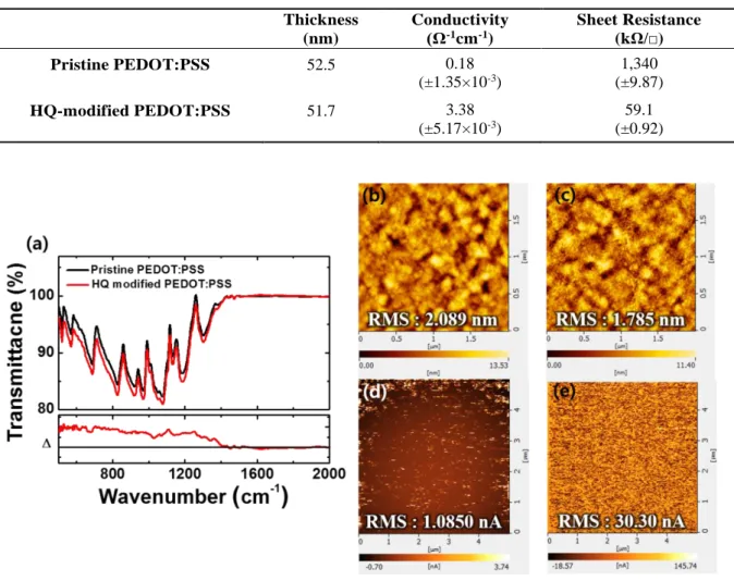
Figure 1.1. Current best research-cell efficiencies in OSCs. ... 1 Figure 1.2. The operational principle of BHJ OSCs. ... 3 Figure 1.3. The binary device structure of bilayer and BHJ. ... 4 Figure 1.4. Schematic of the working mechanisms in ternary organic solar cells. (a) The charge transfer mechanism. (b) The energy transfer mechanism. (c) The parallel like mechanism. (d) The alloy model. ... 6 Figure 1.5. (a) Device structure of tandem solar cells, (b) Simplified band diagram of a tandem cell made of two sub-cells connected in series via an intermediate connection layer. ... 8 Figure 1.6. Schematic illustration of an OSCs with interfacial layer. ... 17 Figure 2.1. (a) Schematic illustration of the device structure and chemical structure of the ph
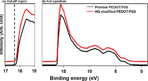
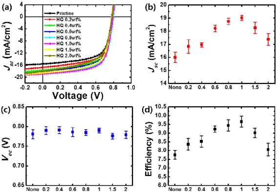
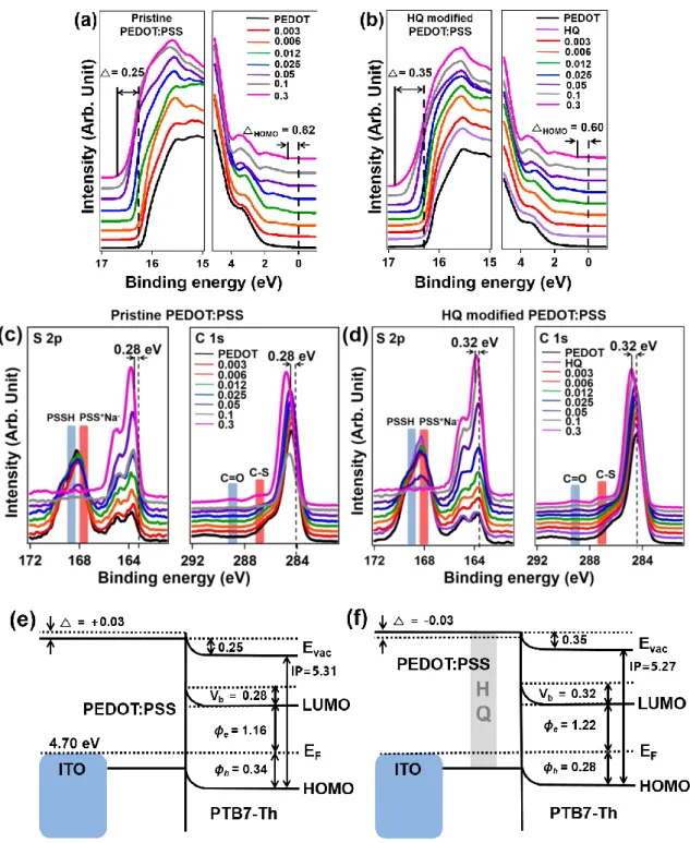
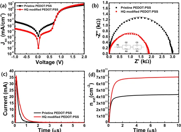
otoactive materials (donor: PTB7-Th, acceptor: PC71BM) and hydroquinone (HQ) surface modifier for PEDOT:PSS, (b) Energy level diagram of a BHJ solar cell based on a PTB7-Th:PC71BM blend. ... 27 Figure 2.2. UPS spectra of pristine PEDOT:PSS and modified PEDOT:PSS on ITO. ... 28 Figure 2.3. (a) J-V characteristics of PTB7-Th:PC71BM solar cells with pristine PEDOT:PSS and PEDOT:PSS modified with various ratios of HQ. (b) Jsc, (c) Voc, and (d) PCE distributions for the solar cells with pristine PEDOT:PSS and PEDOT:PSS modified with various ratios of HQ. The data were obtained from 20 devices for each case. ... 29 Figure 2.4. J-V characteristics of (a) P3HT:PCBM and (b) PTB7:PC71BM solar cells with pristine PEDOT:PSS and HQ modified PEDOT:PSS with various HQ ratios. ... 30 Figure 2.5. Secondary electron cut-off and HOMO onset UPS spectra of (a) pristine PEDOT:PSS and (b) HQ-modified PEDOT:PSS with increasing concentrations of PTB7-Th. The XPS spectra for S 2p and C 1s of (c) pristine PEDOT:PSS and (d) HQ-modified PEDOT:PSS with increasing concentrations of PTB7-Th. Schematic energy-level diagrams of PTB7- Th on (e) pristine PEDOT and (f) HQ-modified PEDOT:PSS. The energy unit is eV. (EF: Fermi energy level, Evac: Vacuum level, Δ: Interfacial dipole, IP: Ionization potential, Vb: Energy level relaxation, φe: Electron injection barrier, φh: Hole injection barrier). ... 33
vi
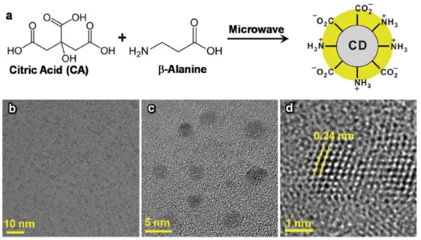
Figure 2.6. (a) Dark J-V characteristics of PTB7-Th:PC71BM solar cells with pristine PEDOT:PSS and HQ-modified PEDOT:PSS. (b) Nyquist plot of impedance spectroscopy measurements at Voc under light irradiation and the corresponding equivalent circuit model. (c) CE current transient under 1 sun Voc conditions. (d) Calculated charge extraction density from the CE measurements. ... 35 Figure 2.7. (a) FTIR absorption spectra of IRAV modes in mid-IR region in pristine PEDOT:PSS and HQ-modified PEDOT:PSS. AFM topo images of (b) pristine PEDOT:PSS and (c) HQ- modified PEDOT:PSS. C-AFM images of (d) pristine PEDOT:PSS and (e) HQ-modified PEDOT:PSS on an ITO substrate in the dark at +3V. ... 36 Figure 3.1. (a) Schematic scheme of CQD synthesis. (b, c) TEM images of CQDs. The typical mean size of the CQDs was 3.1 ± 0.5 nm. (d) HRTEM image showed the arrangement of carbon atoms in CQDs with a lattice spacing of 0.24 nm. ... 43 Figure 3.2. (a) Schematic illustration of the single-junction solar cell structure. (b) J–V characteristics of PTB7-Th:PC71BM single-junction solar cells with pristine PEI and CQD-doped PEI with various doping ratio. Note that the PEI layer in single-junction solar cells was acted as a WF modify layer. (c) EQE spectra of PTB7-Th:PC71BM single-junction solar cells with pristine PEI and CQD-doped PEI with various doping ratio. ... 45 Figure 3.3. (a) J–V characteristics of P3HT:PCBM single-junction solar cells with pristine PEI and CQD-doped PEI with various doping ratio. (b) J–V characteristics of PTB7:PC71BM single-junction solar cells with pristine PEI and CQD-doped PEI with various doping ratio.
In both cases, the optimized CQD doping concentration was 0.5%. ... 47 Figure 3.4. (a) Schematic illustration of the homo-tandem solar cell structure. (b) Cross-sectional TEM images of tandem solar cell with CQD-doped PEI. (c) J–V characteristics of tunnel junction tandem solar cell with and without CQD doping on PEI. J–V characteristics of single- junction solar cells were presented together for comparison. (d) Estimated EQE spectra deduced from total absorption of device and IQE of sub-cells. EQE spectra of single- junction solar cells were presented together for comparison. ... 49 Figure 3.5. (a) Statistical distribution of the efficiency of single-junction cells with pristine PEI layer.
(b) Statistical distribution of the efficiency of single junction cells with CQD-doped PEI layer. (c) Statistical distribution of the efficiency of tunnel junction tandem solar cells with
vii
pristine PEI layer. (d) Statistical distribution of the efficiency of tunnel junction tandem solar cells with CQD-doped PEI layer. ... 50 Figure 3.6. AFM height image (5.0 μm × 5.0 μm) of pristine PEI layer and CQD-doped PEI layer with various doping ratio. ... 51 Figure 3.7. (a) Nyquist plots of impedance spectra for single-junction solar cells with various CQD doping ratio. (b) Nyquist plots of impedance spectra for tandem solar cells with and without CQD doping on PEI. (c) Intensity modulated photovoltage spectroscopy (IMVS) of tandem solar cells with and without CQD doping on PEI. ... 53 Figure 3.8. UPS spectra of (a) CQD doped PEI on PEDOT:PSS, (b) CQD doped PEI on ITO. (c) Work-
function values deduced from UPS spectra. The work-function of PEODT:PSS was significantly reduced with PEI covering. However, CQD doping did not change the modified work-function of PEDOT:PSS. ... 53 Figure 4.1. (a) Schematic diagram of CQD synthesis. (b) TEM images of CQDs. The typical mean
size of the CQDs was 3.6 ± 1.2 nm. (c) HRTEM image showed the arrangement of carbon atoms in CQDs with a lattice spacing of 0.21 nm. ... 58 Figure 4.2. (a) Schematic illustration of device structure used in this study. (b) The J-V characteristics
of PTB7-Th:PC71BM solar cells with pristine PEI and CQD-doped PEI with various doping ratios, (c) EQE curves of PTB7-Th:PC71BM solar cells with pristine PEI and CQD-doped PEI with various doping ratios. ... 60 Figure 4.3. (a) Non-modulated impedance spectroscopy of PTB7-Th:PC71BM solar cells with pristine PEI layer and CQD-doped PEI layer, (b) Charge extraction density of PTB7-Th:PC71BM solar cells with pristine PEI layer and CQD-doped PEI layer, (c) Jsc versus light intensity for PTB7-Th:PC71BM solar cells with pristine PEI layer and CQD-doped PEI layer, (d) Voc
versus light intensity for PTB7-Th:PC71BM solar cells with pristine PEI layer and CQD- doped PEI layer. ... 61 Figure 4.4. (a) Photocurrent density (Jph) versus effective voltage (Veff). (b) J-V measured under dark conditions. ... 63 Figure 4.5. AFM images of the PTB7-Th:PC71BM active layer deposited on pristine PEI layer (left)
and CQD-doped PEI layer (right). ... 64 Figure 4.6. (a) Energy level diagram of PTB7-Th:PC71BM solar cells. The work-functions of ITO, ITO with PEI, and ITO with CQD-doped PEI were measured by Kelvin-probe force microscopy.
(b) Diagram of summarized concept; CQD-doped PEI induced stronger internal field due
viii
to the lower work-function. This strengthened internal field induced better exciton dissociation efficiency. ... 65 Figure 5.1. Schematic illustration of the device structure and chemical structure of the photoactive materials (donor: PBDB-T-2F (also called PM6), acceptor: Y6) and WPFSCz-. ... 71 Figure 5.2. J-V characteristics of PBDB-T-2F:Y6 solar cells made with and without a WPFSCz- layer, based on different types of PEDOT:PSS: (a) AI4083, (b) Clevios P, (c) PH1000, and (d) PH1000 + 5% DMSO. ... 72 Figure 5.3. J-V measurements of PBDB-T-2F:Y6 solar cells based on PEDOT:PSS AI4083, Clevios P,
PH1000, and PH1000 + 5% DMSO, both with and without a WPFSCz- layer. (a) Dark current density (JSC). (b) Photocurrent density (Jph) versus effective voltage (Veff = V0 - V).
... 74 Figure 5.4.(a-d) Jsc versus light intensity for PBDB-T-2F:Y6 solar cells with and without a WPFSCz- layer. (e-h) Voc versus light intensity for PBDB-T-2F:Y6 solar cells with and without a WPFSCz- layer. The device based on (a, e) AI4083, (b, f) Clevios P, (c, g) PH1000, (d, h) PH1000+5% DMSO. ... 75 Figure 5.5. Photovoltage, photocurrent, and impedance spectroscopy measurements of PBDB-T-2F:Y6 solar cells with and without a WPFSCz-layer. (a) Transient photovoltage. (b) Transient photocurrent. (c) Non-modulated impedance spectroscopy. (d) Intensity-modulated photocurrent spectroscopy. (e) Intensity-modulated photovoltage spectroscopy. (f) Trap density vs. trap energy level. ... 77 Figure 5.6. (a) X-ray photoelectron spectra of O 1s peaks obtained from ITO with and without a layer of WPFSCz-. (b) High binding region of ultraviolet photoelectron spectra of ITO with and without a WPFSCz-. (c) The corresponding energy level diagrams. (d) The energy level diagram of the components in the PBDB-T-2F:Y6 solar cells with a WPFSCz-layer. ... 79 Figure 5.7. Surface potential images of (a) ITO, (b) ITO with WPFSCz-, (c) PEDOT:PSS on ITO, (d)
PEDOT:PSS on ITO with WPFSCz-. ... 80 Figure 5.8. (a) The J-V characteristics, (b) EQE curves of PBDB-T-2F:Y6 inverted devices without and with WPFSCz- layer based on MoOx as HTL. ... 81 Figure 5.9. (a) The J-V characteristics, (b) EQE curves of PBDB-T-2F:Y6 inverted devices without and with PFN-Br layer, (c) Voc versus light intensity for PBDB-T-2F:Y6 inverted devices without and with PFN-Br layer. ... 81
ix
List of Tables
Table 1.1. Device characteristics of some representative OSCs with different CIMs and AIMs. .... 22 Table 2.1. Summarized device performance characteristics of PTB7-Th:PC71BM solar cells with pristine PEDOT:PSS and PEDOT:PSS modified with various amounts of HQ. ... 29 Table 2.2. Summarized device performance characteristics of P3HT:PCBM solar cells with pristine PEDOT:PSS and HQ modified PEDOT:PSS with various ratios. ... 31 Table 2.3. Summarized device performance characteristics of PTB7:PC71BM solar cells with pristine PEDOT:PSS and HQ modified PEDOT:PSS with various ratios. ... 31 Table 2.4. Conductivity and sheet resistance of pristine and HQ-modified PEDOT:PSS. ... 36 Table 3.1. Summarized photovoltaic performance characteristics of single-junction solar cells with pristine PEI layer and CQD-doped PEI layer with various doping ratios. ... 45 Table 3.2. Summarized photovoltaic performance characteristics of single junction solar cells fabricated with P3HT and PC61BM as a photoactive layer. ... 47 Table 3.3. Summarized photovoltaic performance characteristics of single junction solar cells fabricated with PTB7 and PC71BM as a photoactive layer. ... 47 Table 3.4. Summarized photovoltaic performance characteristics of single-junction solar cells and tandem solar cells with pristine PEI layer and CQD-doped PEI layer. ... 49 Table 4.1. Summarized photovoltaic performance characteristics of PTB7-Th:PC71BM solar cells with pristine PEI layer and CQD doped PEI layer with various doping ratios. ... 60 Table 4.2. Exciton generation rate (Gmax) and charge separation probabilities (P(E,T)) of PTB7-
Th:PC71BM solar cells with pristine PEI layer and CQD-doped PEI layer. ... 63 Table 5.1. Summarized photovoltaic performance characteristics of PBDB-T-2F:Y6 solar cells with and without a WPFSCz- layer based on various types of PEDOT:PSS. Average PCE values were obtained from 30 devices. EQE Jsc values were calculated from EQE measurements.
... 72 Table 5.2. Summary of exciton generation rate (Gmax) and charge separation probabilities (P(E,T)) of PBDB-T-2F:Y6 solar cells with and without a WPFSCz- layer using different types of
x
PEDOT:PSS. ... 74 Table 5.3. Summarized transit time (trap), recombination time (rec), and charge collection efficiency of PBDB-T-2F:Y6 solar cells made with and without a WPFSCz- layer. ... 77 Table 5.4. Photovoltaic performance characteristics of PBDB-T-2F:Y6 solar cells without and with WPFSCz- layer based on various PEDOT:PSS. ... 81 Table 5.5. Photovoltaic performance characteristics of PBDB-T-2F:Y6 inverted devices without and with PFN-Br layer. ... 81
xi
List of Abbreviations
Abbreviation Description
AFM atomic force microscopy AIM anode interface material
BHJ bulk-heterojunction
CA citric acid
CB chlorobenzene
CF chloroform
CIM cathode interface material
CN 1-chloronaphthalene
CQD carbon quantum dot
DIO 1,8-diiodooctane
EQE external quantum efficiency ETL electron transport layer
FF fill factor
FTIR Fourier-transform infrared spectroscopy Gmax exciton generation rate
HOMO highest occupied molecular orbital
HQ hydroquinone
HRTEM high-resolution transmission electron microscopy HTL hole transport layer
IMPS intensity-modulated photocurrent spectroscopy IMVS intensity-modulated photovoltage spectroscopy
IPA isopropyl alcohol
IQE internal quantum efficiency IS impedance spectroscopy
ITO indium tin oxide
Jph photocurrent density JSC short circuit current
KPFM Kelvin probe force microscope LUMO lowest unoccupied molecular orbital
OSC organic solar cell
P(E, T) exciton dissociation probability
PC71BM [6,6]-phenyl-C71-butyric acid methyl ester PCE power conversion efficiency
PEDOT:PSS poly(3,4-ethylenedioxy-thiophene):poly(styrenesulfonate)
PEI polyethyleneimine
PEIE ethoxylated polyethyleneimine PSC polymer solar cell
PTB7-Th poly[[4,8-bis[5-(2ethy-lhexyl)thiophen-2-yl]benzo[1,2-b:4,5- b0]dithiophene-2,6-diyl][3-fluoro-2-[(2-ethylhexyl)carbo- nyl]thieno[3,4-b]thiophenediyl]]
QY quantum yield
xii
RMS root mean square
SRH Shockley-Read-Hall
TPC transient photocurrent TPV transient photovoltage
UPS ultraviolet photoelectron spectroscopy Veff effective voltage
VOC open circuit voltage
WF work-function
WPFSCz-
9-(2,7-Diethylheptyl)-2,7-bis(4,4,5,5-tetramethyl-1,3,2-dioxaborolan- 2-yl)-9H-carbazole, 2,7-dibromo-9,9-bis(4-sulfonatobutyl) fluorene dipotassium, and potassium poly[9,9-bis(3′-sulfonatopropyl)fluorene- alt-(9-(2,7-diethylheptyl)-carboazole)]
XPS x-ray photoelectron spectroscopy
1
Chapter 1. Introduction
1.1 Organic Solar Cells (OSCs)
1.1.1 History of OSCs
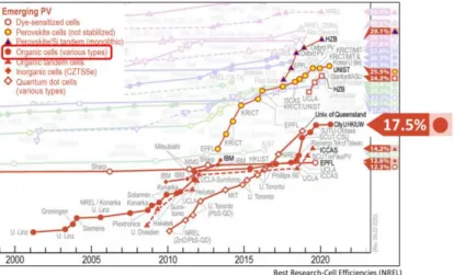
The first example of a conducting polymer Polyacetylene was developed by Hideki Shirakawa, Alan MacDiarmid and Alan Heeger in 1977.1 They tried to improve the conductance and study the polymer system and were able to reach conductivities as high as many metals. Though polyacetylene itself proved to be too difficult to work with and unstable to be used commercially, their discovery lead to an entire field of conducting polymers, including poly(p-phenylene vinylene) (PPV) used in some organic light emitting diode displays and the polythiophene based materials used in OSCs. This work led to them being awarded the 2000 Nobel Prize in Chemistry. A breakthrough occurred in 1986, when Tang showed that much higher efficiencies are attainable by producing a double-layered cell using two different dyes, which had a large photocurrent density, of the order of mA/cm2, and an efficiency of 1%.2 This result had a big impact on the field of organic solar cells. A blended junction for small molecule cells was proposed in 1991 by Hiramoto.3,4 In 1992, Sariciftci reported a polymer heterojunction cell composed of C60 and MEH-PPV (poly[2-methoxy-5-(2-ethylhexyloxy)-1,4- phenylenevinylene]).5 Followed in 1995, a polymer bulk-heterojunction (BHJ) cell reported by Yu.6 After 2000, based on these fundamental studies, the efficiency rose from 1% and started to increase rapidly and reached 17.5% as shown 1.1.7 In recent years, Due to the continuous development of active materials8-12 and device structure engineering, such as tandem, ternary device13-16,and interfacial engineering17-21, Power conversion efficiency (PCE) of OSCs has exceeded 17% by choosing matched donor and acceptor materials in photoactive layer.22
Figure 1.1. Current best research-cell efficiencies in OSCs.
2 1.1.2 Principle of OSCs
The OSC is a type of solar cell where the absorbing layer is based on organic semiconductors, typically either polymers or small molecules. For organic materials to become conducting or semiconducting, a high level of conjugation is required. The electrons associated with the double bonds become delocalized across the entire length of conjugation due to the conjugation of the organic molecule. These electrons have higher energies than other electrons in the molecule and are equivalent to valence electrons in inorganic semiconductor materials.
However, in organic materials, these electrons do not occupy a valence band but are part of what is called the ‘highest occupied molecular orbital’ (HOMO). Also, there are unoccupied energy levels at higher energies just like inorganic semiconductors, it is called the ‘lowest unoccupied molecular orbital’
(LUMO). Between the HOMO and LUMO of the organic semiconductors is an energy gap. With increased conjugation, the band gap will become small enough for visible light to excite an electron from HOMO to LUMO. When the energy of light is equal to or greater than the band gap, leading to absorption and excitation of an electron from the HOMO to the LUMO. The excited electron will leave behind a positively charged space known as a hole. Due to the opposite charges of the hole and electron, they become attracted and form an electron-hole pair, also known as an exciton. The OSCs have low dielectric constants, giving large exciton binding energy values in the range of 0.3-0.7 eV.23 Because the exciton cannot be dissociated by thermal energy alone, at least two different organic semiconductors are needed. The energy levels between the two different organic semiconductors are offset, with the difference being greater than exciton binding energy, allowing exciton dissociation to occur at the interface between them. Depending on electron has been donated by a material, or accepted by a material, the organic semiconductors are classified as either a donor or acceptor.
3
The working principle of OSCs can be summarized four steps which required for generation of electrical power via the absorption of incident light:
i) Absorption of photons and formation of photo-induced excitons in donor and acceptor, respectively.
ii) The excitons diffusion and dissociation at the donor and acceptor interface.
iii) Charge-transfer (CT) states generation and then dissociation into free charge carriers (electrons and holes) with an ultrafast quasi-adiabatic charge transfer process.
iv) Charge carriers that are transported through either donor and acceptor and then being collected by the respective electrodes transfer process.
Figure 1.2. The operational principle of BHJ OSCs.
The separated charge carriers may recombine with each other (geminate recombination) before dissociation. Moreover, the separated charge carriers may also be recombined (bimolecular recombination or non-geminate recombination) before collected by the respective electrodes. The germinate and non-germinate recombination have a great effect on the low PCEs in BHJ OSCs.
4
1.1.3 Structures of OSCs 1.1.3.1 Bilayer & BHJ OSCs
C. W. Tang introduced the world's first two-layer thin-film solar cell with an efficiency of 1% in 1986.1 In the bilayer structure, a transparent electrode ITO is used as an anode, and a metal having a low work-function is used as a cathode, and a donor material and an acceptor material are stacked as a photoactive layer between them as shown in Figure 1.3a. However, since it only takes about 100 ps for the holes and electrons of excitons to recombine, the exciton diffusion length is only about 10 nm. There is a limit to the contact area between them, revealing a limit to the formation of free holes and electrons.
To overcome this limitation, a BHJ structure which a donor material and an acceptor material are properly mixed has been developed. As shown in Figure 1.3b, it has the advantage of improving photovoltaic conversion efficiency because the interface between the photoactive layer is wide. If the donor and acceptor form a heterojunction structure in the nanometer region within the photoactive layer, excitons excited by light absorbed by the photoactive layer will be separated into free electrons and holes in the adjacent p-n junction region. For excitons to be separated into free electron-holes at the p- n junction interface, the difference between the LUMO or HOMO energy levels of the two materials must be greater than the exciton binding energy. The electrons and holes separated at the many p-n junction interfaces distributed throughout the photoactive layer diffuse and flow to both electrodes along the donor and acceptor respectively to form photocurrents. Therefore, it is important that the donor and acceptor have proper phase separation in the nanometer region in order to separate electrons and holes and transfer to both electrodes. In 1995, A. J. Heeger group announced that BHJ structure solar cell greatly helps to improve efficiency as a solution process that has a much lower process cost compared to vacuum deposition.24 Currently, OSCs with an efficiency approaching 18% are fabricated by a simple spin-coating method, and the BHJ structure is widely used in OSC research.
Figure 1.3. The binary device structure of bilayer and BHJ.
5 1.1.3.2 Ternary OSCs
Despite significant advances in binary BHJ cells, the PCE of OSCs needs to be further boosted to realize practical applications and commercialization. However, their performance is restricted by the insufficient coverage of the solar spectrum of binary blends because of the intrinsic narrow absorption bands of organic semiconductors. On the other hand, as organic molecules typically present low charge carrier mobility, BHJ films usually retain very thin (as low as 100 nm) to gain efficient charge collection, unfortunately, which cannot fully capture all incident sunlight in their absorption ranges.25 Recently, a ternary OSCs incorporating a simple process of a single-junction OSCs has been in the limelight having the advantage of minimizing the thermalization loss and a wide absorption area of the tandem OSCs.
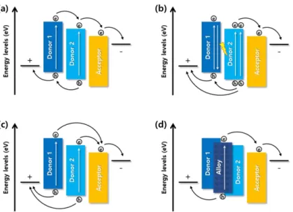
The ternary OSCs consisting of three light absorbing materials (a donor, an acceptor, and an additional third component donor or acceptor) in one photoactive layer. And the third component plays a crucial role in improving the film morphology, facilitating exciton dissociation, and enhancing charge transport of binary BHJ cells. Accordingly, ternary OSCs have been investigated to further increase the PCE of OSCs. According to the functionality of the third component, it can be classified into four categories:
charge transfer, energy transfer, parallel-like, and alloy model as shown in Figure 1.4. The third component is limited to the donor material in Figure 1.4. Even if the acceptor material becomes the third component, the charge transport mechanism is the same.26
In case of charge transfer mechanism as shown in the Figure 1.4a, the third component locates at the interface of the main donor and acceptor that transfers the charge to the electrode with forming cascade energy levels alignment. That is, holes generated at the donor 1 and acceptor interface are directly extracted to the anode, and electrons are extracted to the cathode through donor 2 and acceptor. On the other hand, holes generated at the donor 2 and acceptor interface pass through donor 1 to the anode, and electrons are collected directly to the cathode. Thus, the observed VOC of such systems is basically fixed to the smaller VOC of the original binary systems. In the energy transfer mechanism as shown in the Figure 1.4b, the big difference from other mechanism is that the emission spectrum of the third component needs to substantially overlaps with the absorption spectrum of the primary donor or acceptor. In other words, there is an energy donor that transfers energy without generating a charge carrier and an energy acceptor that not only absorbs light by itself, but also absorbs the light emitted by the energy donor to generate charge carrier. The location of the energy donor within the photoactive layer should be near the energy acceptor due to the limited energy transport distance. If the energy transfer mechanism of the donor 1, donor 2 and acceptor-based ternary OSC is applied, the exciton energy of donor 1 is transferred to donor 2 through Förster or Dexter energy transport, and the excitons generated in donor 2 are separated at the donor 2 and acceptor interface and creates charge carrier. The generated electrons are collected along acceptor to the cathode, and holes are extracted to the anode
6
through donor 1 or directly to the anode according to the relative HOMO energy level position of donor 1. Therefore, similar to the charge transport mechanism, the change in the VOC is insignificant. The following parallel-like mechanism or alloy model, two binaries operate independently as one photoactive layer without requirements such as morphology, energy level, and band gap of the ternary photoactive layer. In other words, in a donor 1, donor 2 and acceptor-based ternary organic solar cell, when a parallel-like or alloy model is applied, holes and electrons generated at the donor 1 and acceptor interface are directly collected to the anode and cathode along each pathway. In addition, holes and electrons generated at the donor 2 and acceptor interface are also independently extracted directly to each anode and cathode. Therefore, in parallel-like or alloy model, the VOC of the ternary OSC is determined by the ratio of the ternary photoactive material. In the parallel-like mechanism, When the donor 2 absorbs light, splits excitons and transports holes, that is, the third component forms its own independent hole-transport network. In this case, the VOC values of ternary OSCs lie between the measured values of the two individual binary cells and it depends on the composition of the ternary mixture, rather than being fixed by the LUMO energy levels of the acceptors or the HOMO energy levels of the donors (Figure 1.4c). Unlike the parallel-like mechanism, the Alloy Model, on the other hand, is electronically coupled between two photoactive materials to form a new charge-transfer (CT) state energy which would require a good miscibility and compatibility of the donor materials as shown Figure 1.4d. The CT state energy in such a system was shown to be a function of the ternary blend composition and followed the shift in VOC.27
Figure 1.4. Schematic of the working mechanisms in ternary organic solar cells. (a) The charge transfer mechanism. (b) The energy transfer mechanism. (c) The parallel-like mechanism. (d) The alloy model.
7 1.1.3.3 Tandem OSCs
The single-junction BHJ OSCs have achieved a significant improvement of over 17% power conversion efficiency through the synthesis of highly effective polymer or small molecule materials and device development, but due to a narrow absorption area (~120nm), low exciton diffusion length with low charge carrier mobility (~10-5 cm2 /Vs) and thermalization loss, it is difficult to expect further efficiency improvement for single-junction OSCs. The research on a tandem OSCs has been studied to realizing high performance organic solar cells by overcome this problem. The working principle of the tandem cell is as follows. First, excitons are formed by absorption of light in the top and bottom cells.
Second, after excitons are separated from each cell, holes in the bottom cell collect electrons in the top cell and recombine near the intermediate layer. Although the described working principle is based on an inverted tandem OSCs, the principle is the same only the direction of the charge carrier is opposed in the conventional structure.28-29
In tandem OSCs, as shown in Figure 1.5a, independent single-junction organic solar cells are physically separated by an intermediate layer and can be connected either in series or in parallel depending on the nature of the intermediate layer and on the way the intermediate layer and the two electrodes are connected. Normally, the series connection is widely used. The tandem OSCs can be roughly divided into hetero-tandem OSCs and HOMO-tandem OSCs. The hetero-tandem OSCs is a wide-bandgap material for the bottom cell in combination with a narrow-bandgap material for the top cell with complementary absorption spectra and minimal absorption overlap and The HOMO-tandem OSCs is a same donor material for both sub-cells that comprise high internal quantum efficiency (IQE) in single cells with high PCEs. In the overall tandem OSCs, the thickness of the photoactive layer of each sub-cell is optimized by the light absorption coefficient, band gap, and charge mobility of the photoactive layer. In general, the thickness of the photoactive layer in the bottom cell is thinner than that of the top cell.
The energetic diagram of the device can be represented as in Figure 1.5b. In tandem OSCs, intermediate connection layers (ICLs) plays an important role in the overall device characteristics. The ICLs generally consist of a p-type hole transporting layer (HTL) and an n-type electron transporting layer (ETL) and should allow the recombination of holes coming from one sub-cell with electrons coming from the other. In the ICLs, the vacuum level which driven by the alignment of fermi levels of the HTL and ETL is simultaneously shifted. To satisfied ideal ICLs, it should be highly transparent and robust enough to protect underlying layers, and they should form ohmic contact with sub-cell photoactive layers to ensure efficient charge extraction. Therefore, The ICLs optically and electrically connects the sub-cell and also, the formation of HTL and ETL of ICLs is very important because
8
improves optical field distribution and charge transfer collection to top cell are different depending on which HTL and ETL are used for ICL. Since the tandem OSC is connected in series of bottom cell and top cell, the VOC of the tandem OSC is equal to the sum of the VOC of the two sub-cells. However, JSC
appears smaller than each cell. This is because the current value in the tandem OSCs has the current of the sub-cell having a small current, where the light absorption of the top cell absorbs light that has not been absorbed by the bottom cell, the top cell generally generates a relatively low current value because it absorbs light with a lower intensity. Even though the fabrication method is more complicated than the other structure such as binary and ternary structures, and there is a disadvantage that the material for ICLs can be limited by annealing process, still has a high possibility that high efficiency tandem OSCs can be achieved by more efficient new materials, functional intermediate layers and better matching of the materials with complimentary absorption spectra.30
Figure 1.5. (a) Device structure of tandem solar cells, (b) Simplified band diagram of a tandem cell made of two sub-cells connected in series via an intermediate connection layer.
9
1.2 Characterization of OSCs
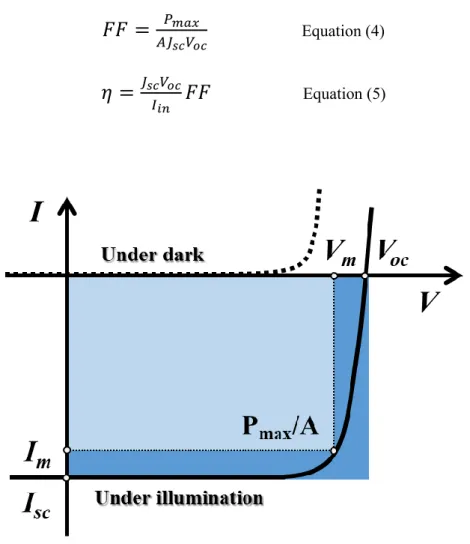
1.2.1 DeviceCharacterization
The fundamental electrical characterization of a photovoltaic diode is carried out by obtaining curves of electric current density vs. an external voltage (bias), the so-called J-V curves. The J-V curve is one of the most common methods of determining how an electrical device functions in a circuit. A typical J-V curve for a solar cell is shown in Figure 1.3, in the dark and under illumination. The photocurrent density Jph is a subtraction between the two J-V curves (illuminated and dark), which are described by the Equations (1) and (2), where Jo is the reverse dark current, V is the bias voltage, n is the diode quality factor, k is the Boltzmann constant and T is the temperature.
𝐽(𝑉) = 𝐽0[(𝑒𝑉
𝑛𝑘𝑇) − 1] (𝑆ℎ𝑜𝑐𝑘𝑙𝑒𝑦′𝑠 𝑒𝑞𝑢𝑎𝑡𝑖𝑜𝑛) Equation (1) 𝐽(𝑉) = 𝐽0[(𝑛𝑘𝑇𝑒𝑉) − 1] + 𝐽𝑝ℎ (𝑢𝑛𝑑𝑒𝑟 𝑖𝑙𝑙𝑢𝑚𝑖𝑛𝑎𝑡𝑖𝑜𝑛) Equation (2)
The parameters that characterize solar cells in general are shown in Figure 1.3, the short-circuit current density (Jsc), the open-circuit voltage (Voc) and the maximum operating power (Pmax), which determine the fill factor (FF).31
The short circuit current density (Jsc) is the current that flows when there is no external field applied;
the charges are drifting because of the internal field. Jsc is determined by the number of photons absorbed (the number of photoexcitations), the quantum efficiency for charge separation, and the transport of the charge carriers through the material. A broad absorption spectrum is advantageous, for one wants to harvest as large a fraction as possible of the photons from the broad spectrum of the sun.
The open circuit voltage (Voc) is defined as the maximum voltage that is obtained when no current is generated by the solar cell. VOC is determined by the difference in the quasi-Fermi levels of the phase.
The open circuit voltage is given by Equation (3).
𝑉𝑜𝑐 ≈ 𝐸𝑎𝑐𝑐𝑒𝑝𝑡𝑜𝑟(𝐿𝑈𝑀𝑂)+ 𝐸𝑑𝑜𝑛𝑜𝑟(𝐻𝑂𝑀𝑂)+ 𝑘𝐵/𝑒{ln (𝑛𝑒𝑛ℎ/𝑁𝑐2)} Equation (3)
where n e and n h are the electron and hole densities, respectively and Nc is the corresponding density of states near the acceptor lowest unoccupied molecular orbital (LUMO) and the donor highest occupied molecular orbital (HOMO), assumed to be equal. However, the excellent correlation required the addition of an additional 0.3 eV of unknown origin and it directly from the third term in Equation 1. In principle, Voc can be increased by the difference in work functions of the anode and cathode. However, the use of interlayers (electron transport/hole blocking and hole transport/electron blocking) tends to decouple the Voc from the difference in the anode and cathode work functions.32
10
The fill factor (FF) is determined by the competition between sweep-out of the photogenerated carriers and the recombination of carriers to the ground state. Normally, The FF is defined as the ratio of the maximum operating power (Pmax) to the maximum extractable power from an ideal solar cell, which would be the product of the device area A, Voc, and Jsc.
Thus, the power conversion efficiency is the ratio of the maximum operating power Pmax to the input power of the incident light on the solar cell. Therefore, under an incident light intensity Iin, the FF and the power conversion efficiency (η) are given by Equations (4) and (5).
𝐹𝐹 =
𝑃𝑚𝑎𝑥𝐴𝐽𝑠𝑐𝑉𝑜𝑐
Equation (4)
𝜂 =
𝐽𝑠𝑐𝑉𝑜𝑐𝐼𝑖𝑛
𝐹𝐹
Equation (5)Figure 1.3. The current-voltage characteristics of a solar cell and the photovoltaic parameters.
11
The quantum efficiency (QE) measurement is critical for material research and device analyzation to understand the conversion efficiency as a function of the wavelength of light. The QE of a solar cell which referred to as incident photon to charge carrier efficiency (IPCE) indicates the ratio of the number of photons incident on device to the number of generated charge carriers. In other word, the QE is defined as the ratio of the number of electrons in the external circuit produced by an incident photon of a given wavelength. The two types of QEs are often considered: external quantum efficiency (EQE) and internal quantum efficiency (IQE). They differ in the treatment of photons reflected from the device.
All photons effect on the device surface are considered in the value of the EQE but only photons that are not reflected are considered in the value of IQE.
The external quantum efficiency (EQE) defined as the number of electrons generated by light in the external circuit divided by the number of incident photons as a function of excitation wavelength. Thus, EQE is often useful tool for look at the quantum efficiency of the light left after the transmitted and reflected light has been lost. The EQE is given by Equation (6). Also, because JSC can be calculated by integrating the EQE curve of overall wavelength using Equation (8), the JSC obtained through the EQE measurement can be confirmed whether JSC obtained from the illuminated IV curve is the correct value.
The internal Quantum Efficiency (IQE) refers to the efficiency with which photons that are not reflected or transmitted out of the device can generate collectable carriers. The IQE curve can be corrected to obtain the EQE curve by measuring the transmission and reflection of device. The IQE is given by Equation (7).
𝐸𝑄𝐸 =𝑒𝑙𝑒𝑐𝑡𝑟𝑜𝑛𝑠/𝑠𝑒𝑐
𝑝ℎ𝑜𝑡𝑜𝑛𝑠/𝑠𝑒𝑐 = (𝑐𝑢𝑟𝑟𝑒𝑛𝑡)/(𝑐ℎ𝑎𝑟𝑔𝑒 𝑜𝑓 𝑜𝑛𝑒 𝑒𝑙𝑒𝑐𝑡𝑟𝑜𝑛)
(𝑡𝑜𝑡𝑎𝑙 𝑝𝑜𝑤𝑒𝑟 𝑜𝑓 𝑝ℎ𝑜𝑡𝑜𝑛𝑠)/(𝑒𝑛𝑒𝑟𝑔𝑦 𝑜𝑓 𝑜𝑛𝑒 𝑝ℎ𝑜𝑡𝑜𝑛) Equation (6) 𝐼𝑄𝐸 = 𝑒𝑙𝑒𝑐𝑡𝑟𝑜𝑛𝑠/𝑠𝑒𝑐
𝑎𝑏𝑠𝑜𝑟𝑏𝑒𝑑 𝑝ℎ𝑜𝑡𝑜𝑛𝑠/𝑠𝑒𝑐=1−𝑅𝑒𝑓𝑒𝑙𝑐𝑡𝑖𝑜𝑛𝐸𝑄𝐸 Equation (7)
𝐽𝑠𝑐 = 𝑞 ∫ Φ(λ)EQE(λ)dλ Equation (8)
The QE depends on the absorption of light and the collection of charges, thereby, charge recombination leads to a decrease in the QE. Therefore, the recombination at the interface should be minimized to obtain improved QE.
12
1.2.2 Data Characterization Techniques 1.2.2.1 Light intensity Dependence Jsc & Voc
The recombination in the device causes loss of photogenerated charge carriers, which is one of the factors that reduce the JSC and FF of the device. Shockley and Queisser showed that VOC of OSC is at its maximum when the photogenerated charges recombine only radiatively. However, the recombination mechanism in BHJ OSCs is mostly non-radiative which mainly affects OSCs includes monomolecular and bimolecular recombination. So, it is important to understand these recombination mechanisms to improve the performance of OSCs. The monomolecular recombination historically refers to either Shockley-Read-Hall (SRH) recombination or geminate recombination. SRH recombination is a first order recombination process in which one electron and one hole recombine through a trap state or recombination center.33 The impurities in the donor and acceptor materials and incomplete phase separation which interfacial defects that act as traps are contributed to a trap-assisted recombination.
That is, if the electrons are trapped in a short time, they provide a fixed place for the holes to recombine.
The light intensity dependence measurement performed by simply changing the incident light intensity using various neutral density filter. The J-V characteristics were collected while illuminating the solar cells over a range of intensities from 1.4 mW/cm2 to 100 mW/cm2. As the incident light intensity decreases, the generated photocurrent also decreases. And at low light intensity, trap sites which present inside the device can more influence on the photocurrent. By fitting JSC vs. light intensity and VOC vs. light intensity, the information of bimolecular recombination and monomolecular (trap- assisted) recombination can be obtained. JSC is proportional to light intensity(I), JSC ∝ Iα. With log-log scale a plot of JSC vs. light intensity which fit to a power law, if fitting line nearly linear dependence as α=1, it means this system is not dominant to bimolecular recombination. On the other hand, it means that carrier losses which originated from bimolecular recombination is existed. VOC is expressed by δVOC=(kBT/e) ln(I), where kB is the Boltzmann constant, T is the absolute temperature and e is the electron charge. The slope of δVOC vs. ln(I) demonstrates that bimolecular recombination dominates for applied voltages near VOC to light intensity. That is, slope S of VOC versus the logarithm of light intensity being equal to kT/q. If slope of fitting line of VOC vs. light intensity is higher than kBT, it means that additional trap-assisted recombination is existed.34
13 1.2.2.2 Trap Density
The electrical characterization techniques are necessary to understand the factors limiting charge transport in these systems, which is usually limited by the low mobility of charge carriers and by trapping effect of defects. Among the technique, admittance spectroscopy technique has been used for investigation for the density of defect states within the OSCs. Admittance spectroscopy is measuring the contribution of the traps by passing from the low frequency to high frequency. With combine admittance spectroscopy to capacitance voltage measurement, the main electrical characterizations which have been performed on these samples were, C-V at room temperature and admittance spectroscopy (C-f). The capacitance voltage and admittance spectroscopy measurements were carried out using impedance analyzer (IVIUM Tech., IviumStat) in the frequency range 100-106 Hz.
In the measurement, the junction capacitance will show a dependence on the measurement frequency.
In this case, the measured capacitance frequency dependence C(ω) is given by Equation (9).
𝐶(𝜔) = 𝐶𝑑+ 𝐶𝑡(𝜔) Equation (9)
The Cd is the frequency independent depletion capacitance and Ct(ω) is the frequency dependent contribution of trap level.
The contribution of one single defect level to the capacitance can be given by Equation (10).
𝐶(𝜔) = 𝐶ℎ𝑓+ 1
1+𝜔2𝜏2(𝐶𝑙𝑓− 𝐶ℎ𝑓) Equation (10)
The Chf is high frequency capacitance which is the depletion capacitance Cd and Clf is the combined contribution of the deep defect and the depletion capacitance. And the contribution of trap Ct is thus given by Chf - Clf, and the dynamics of trap are described by the time constant τ in Equation (11).
𝜏 = (2𝜔0)−1exp ( 𝐸
𝑘𝐵𝑇) Equation (11)
where E is the depth of the state above Ev or below Ec and ω0 is an attempt-to-escape frequency.
The condition ωτ=1 determines the trap level Eω with respect to the valence band maximum is given by Equation (12).
𝐸𝜔= 𝑘𝑇𝑙𝑛(2𝜔0
𝜔 ) Equation (12)
14
To determine the energetic distribution of traps Nt(Eω) from the measured capacitance frequency data C(ω,T). The trap density of states at energy Eω is related to the derivative of the capacitance with respect to the frequency as given by Equation (13).
𝑁𝑡(𝐸𝜔) = −𝑉𝑏𝑖
𝑞𝐿 𝑑𝐶 𝑑𝜔
𝜔
𝑘𝐵𝑇 Equation (13) The Vbi is the built-in voltage and L is the thickness of photoactive layer.35
The traps are generally classified as shallow traps, and deep traps for both electron and hole. If traps are very close to the conduction band (LUMO) within energy bandgap, then traps are classified as shallow traps for electrons. Similarly, if traps located around valence band (HOMO) within energy bandgap, then traps are identified as shallow traps for holes. On the other hand, deep traps of electron and holes are existing far away from LUMO and HOMO level, respectively. The trap density according to energy can be calculated from the following equations measured by admittance spectroscopy (C-V and C-f). By varying the trap energy for frequency‐domain analysis of admittance spectroscopy, it is possible to differential between shallow and deep traps for OSCs.
15 1.2.2.3 Photocurrent Density vs Effective Voltage
From J-V characteristics in a wide reverse bias range under 1 sun illumination, by plotted the results using the net photocurrent (Jph) and the dependence on the effective applied voltage (Veff), it gives further understand of the charge extraction process. The exciton generation rate (Gmax) and exciton dissociation probability (P(E, T)) also can obtain from plotted Jph-Veff results. Jph can expressed by Jph = JL – JD and JL and JD are the current density under illumination and in the dark, respectively. Veff also expressed by Veff =V0-V and V is the applied voltage and V0 is the voltage at which Jph = 0.
If Jph saturated at a large reverse voltage (Veff > 1.5 V), it suggests that all the photogenerated excitons are dissociated into free carriers and all of the carriers are collected at the electrodes without any bimolecular recombination. In this case, saturation current density (Jsat), is only limited by the absorbed incident photo flux, Nphoton. This means that the maximum obtainable Gmax are essentially the same in devices under 1 sun illumination. Gmax can calculated by Jsat=eGmaxL where L is the thickness of the photoactive layer. Using Jsat, P(E, T) can obtain to the ratio of Jph/Jsat. This ratio is essentially the product of the exciton dissociation efficiency and the charge collection efficiency, a decreased Jph/Jsat suggests either a reduced exciton dissociation efficiency or a reduced charge collection efficiency. A reduced charge collection efficiency would suggest that bimolecular recombination begins to dominate. This usually leads to lower FF.36
16
1.3 Interface Engineering
The power conversion efficiency of OSCs is as a result of four processes that occur with the device:
generation of excitons, diffusion of excitons to an donor and acceptor interface, generation of holes as a result of charge separation and transport and collection of charge carriers. Apart from these four processes, the quality of the interface materials is another crucial factor to be considered because they are responsible for facilitating good contact. A typical OSC has a light absorbing BHJ between two electrodes. Interface materials are placed between the photoactive layer, donor and acceptor materials, and the electrode materials as shown in Figure 1.6. Interfaces play an important role in the maintenance of proper contact between photoactive layers in an organic solar cell. The interfacial layer placed between donor and acceptor materials and the electrode and from interfacial engineering, used to achieve ohmic contact at the organic and metal interface. Also the interfacial layer form a selective contact preventing the oppose charge carriers and excitons from recombining at the electrodes thereby enhancing charge extraction property. In addition, the interface materials act as protective layers which prevent the penetration of substance causing problems in OSC stability.
The electrons and holes separated at the BHJ interface where organic semiconductor donors and acceptor materials are irregularly mixed must reach each electrode efficiently to form an external circuit.
To this end, the contact of the organic semiconductor/electrode becomes an important factor that determines the performance of the OSC. The electrical barrier of a few tens of meV of organic semiconductors and metals unfavorable affects OSC characteristics due to significant charge accumulation at the interface and reduction in built-in electric field. Therefore, ohmic contact between each electrode and the organic photoactive layer and selective and efficient charge collection at each electrode are essential. Such methods include the conducting polymers, polymer/polyelectrolytes, fullerene derivatives, or metal oxides.
Another important role of the interfacial layer is to reduce unnecessary energy loss in the OSC structure by matching the energy levels between layers, and to efficiently move charges by increasing the built-in electric field within the device. And to extract. In addition, it is possible to prevent charge recombination occurring at the interface by improving the selective charge collection ability in each electrode, and to form an appropriate morphology of the upper organic photoactive layer by controlling the surface energy of the lower layer. On the other hand, the interfacial layer inserted between the organic photoactive layer/electrode acts as an optical spacer and induces a plasmonic effect to improve exciton generation and charge transport by controlling the optical properties of the organic photoactive layer.
17
By controlling the energy difference, the VOC is increased, or the collection efficiency of electrons is increased to improve the current density JSC and the FF. There are essential requirements that the interfacial layer must have in an OSC based on a solution process. First, when applying the organic photoactive layer solution, the bottom interfacial layer should not have solubility in the organic solvent.
Second, it is necessary to efficiently high light transmittance to the organic photoactive layer. last, the energy level of materials must be considered to enhance the charge transfer capability and charge mobility.31,37
Figure 1.6. Schematic illustration of an OSCs with interfacial layer.
18 1.3.1 Metal Oxides
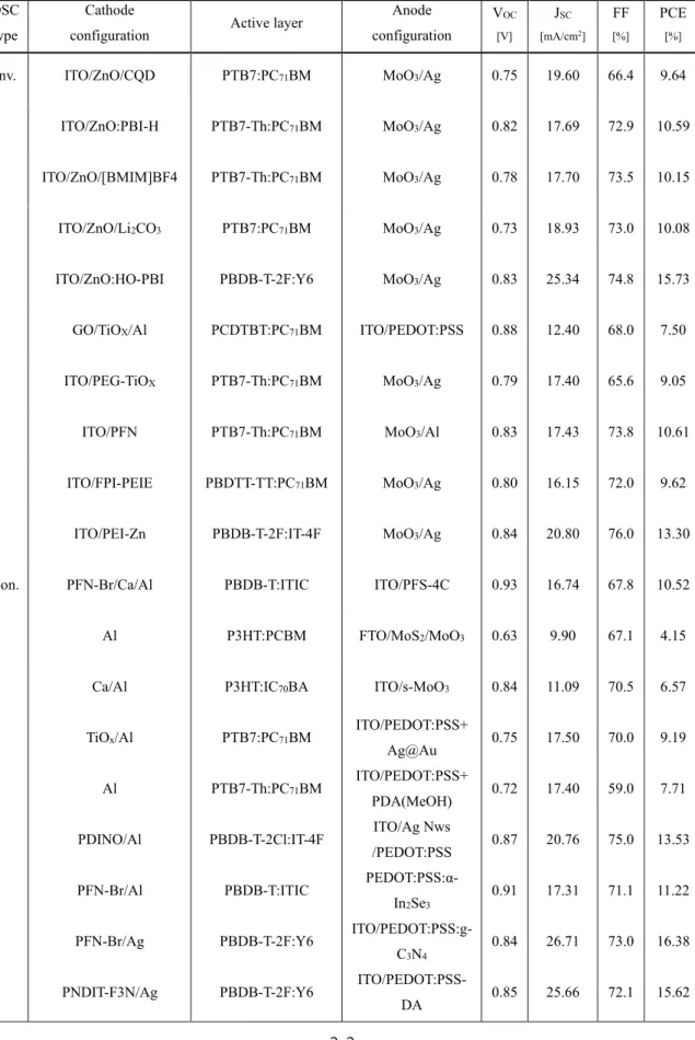
First, ZnO is an inorganic n-type semiconductor, it is commonly used in metal oxide cathode interface materials (CIMs) due to it has a property such as low cost, easy synthesis, non-toxicity, high stability, and unique optical/electronic properties. Generally, ZnO materials have a low WF around 4.3 eV, which offers a proper energy level to reduce WF of ITO or metal electrodes, and to match with LUMO levels of various acceptors such as fullerene-based acceptor and non-fullerene acceptor.38,39 When synthesizing not only ZnO films but also other cathode interface materials, oxygen vacancy may occur depending on the film fabrication condition. By reducing oxygen vacancy through various interface treatments, charge traps can be reduced, and electrical properties can be improved. Therefore, property control of ZnO CIMs to balance their transmittance, electron mobility and interfacial properties, is critical for high performance OSCs.
Zhang et al. applied a bilayer ZnO/CQD as electron extraction layer and it shown that bilayer ZnO/CQD leading to enhanced exciton dissociation, reduced charge recombination and more efficient charge extraction probability, and thereby achieving significant improvement in power conversion efficiency (PCE) of 9.64%.40 By using a dye to modify inorganic ZnO, Nian et al. reported a highly photoconductive CIM for inverted OSCs. This hybrid CIM was achieved by doping a small amount of light absorber such as PBI-H into a sol-gel-derived ZnO, where the PBI-H molecules could form a N−Zn bond with ZnO during the thermal treatment. As a result, the inverteGod devices based on ZnO:PBIH increased from 8.45% to 10.59% for the PTB7-Th:PC71BM system.41 Moreover, Yu et al.
reported that as an ion-liquid of 1-butyl-3-methylimidazolium tetrafluoroborate ([BMIM]BF4) was used to modify ZnO, the [BMIM]BF4-modified ZnO device showed increased JSC and FF as a result of the reduction in the WF of the cathode because the modified ZnO can form spontaneous dipolar polarization at the interface. The PCE of the device using the [BMIM]BF4-modified ZnO CIM was increased to 10.15% in comparison with a PCE of 8.94% for the reference device based on the regular ZnO CIM. 42 By doping the ZnO ripple layer with various metal-carbonate materials, Nho et al. reported the improvement of the performance of the inverted structure organic solar cell. Doping of various metal carbonates in the ZnO ripple layer is formed as a vertical gradient, the work function of the ZnO layer and the LUMO level of PC71BM are properly match. So, it induces improvement in device performance, by preventing electron-hole recombination at the interface.43 Moreover, Wen et al. reported that introduction of four hydroxy (HO) groups into the two perylene bisimide (PBI) bay areas, new HO‐PBI ligands were obtained which upon deprotonation can complex Zn2+ ions and photosensitize semiconductive zinc oxide thin films. Supported by the photoconductive effect of the ZnO:HO‐PBI hybrid interlayers, improved electron collection and transport properties are achieved, leading to remarkable power conversion efficiencies of up to 15.95 %.44