Area-selective external light extraction for metal
bus equipped large area transparent organic
light-emitting diodes
Byoung-Kuk Kang,1, 2 Hyunsu Cho,1 Jun-Han Han,1 Jin-Wook Shin,1 Jinouk Song,3 Seung Koo Park,1 Jonghee Lee,1 Chul Woong Joo,1 Eunhye Kim,3 Seunghyup Yoo,3
Jeong-Ik Lee,1 Byeong-Kwon Ju,2 and Jaehyun Moon1,*
1Soft I/O Interface Research Section, Electronics and Telecommunications Research Institute (ETRI), Daejeon 34129,
South Korea
2Display and Nanosystem Laboratory, College of Engineering, Korea University, Seoul, 02841, South Korea 3Department of Electrical Engineering, Korea Advanced Institute of Science and Technology (KAIST), Daejeon
34141, South Korea
Abstract: Area-selective external light extraction films based on wrinkle structured films were applied to large transparent organic light-emitting diodes (TOLEDs) with auxiliary metal buses. To be specific, on the external surface of the glass, we selectively formed a wrinkle structured film, which was aligned to the auxiliary metal electrodes. The wrinkle-structured film was patterned using a photo-mask and UV curing, which has the same shape of the auxiliary metal electrodes. With this area-selective film, it was possible to enhance the external quantum efficiencies of the bottom and top emissions TOLEDs by 15.7% and 15.1%, respectively, without significant loss in transmittance. Widened angular luminance distributions were also achieved in both emissions directions.
©2016 Optical Society of America
OCIS codes: (250.0250) Optoelectronics; (250.3680) Light-emitting polymers; (220.0220) Optical design and fabrication; (220.4000) Microstructure fabrication.
References and links
1. B. Chen, X. W. Sun, and S. Tan, “Transparent organic light-emitting devices with LiF/Mg:Ag cathode,” Opt. Express 13(3), 937–941 (2005).
2. D. Zhang, K. Ryu, X. Liu, E. Polikarpov, J. Ly, M. E. Tompson, and C. Zhou, “Transparent, conductive, and flexible carbon nanotube films and their application in organic light-emitting diodes,” Nano Lett. 6(9), 1880– 1886 (2006).
3. J. Moon, J. W. Huh, C. W. Joo, J.-H. Han, J. Lee, H. Y. Chu, and J.-I. Lee, “Transparent organic LEDs for new lighting applications,” SPIE Newsroom 5197, 1-3 (2013).
4. G. W. Kim, R. Lampande, J. Boizot, G. H. Kim, D. C. Choe, and J. H. Kwon, “An efficient nano-composite layer for highly transparent organic light emitting diodes,” Nanoscale 6(7), 3810–3817 (2014).
5. R. Meerheim, M. Furno, S. Hofmann, B. Lüssem, and K. Leo, “Quantification of energy loss mechanisms in organic light-emitting diodes,” Appl. Phys. Lett. 97(25), 253305 (2010).
6. K. Hong and J.-L. Lee, “Recent developments in light extraction technologies of organic light emitting diodes,” Electron. Mater. Lett. 7(2), 77–91 (2011).
7. W. H. Koo, W. Youn, P. Zhu, X.-H. Li, N. Tansu, and F. So, “Light extraction of organic light emitting diodes by defective hexagonal-close-packed array,” Adv. Funct. Mater. 22(16), 3454–3459 (2012).
8. M. Slootsky and S. R. Forrest, “Enhancing waveguided light extraction in organic LEDs using an ultra-low-index grid,” Opt. Lett. 35(7), 1052–1054 (2010).
9. W. H. Koo, S. M. Jeong, F. Araoka, K. Ishikawa, S. Nishimura, T. Toyooka, and H. Takezoe, “Light extraction from organic light-emitting diodes enhanced by spontaneously formed buckles,” Nat. Photonics 4(4), 222–226 (2010).
10. D.-H. Cho, J.-W. Shin, J. Moon, S. K. Park, C. W. Joo, N. S. Cho, J. W. Huh, J.-H. Han, J. Lee, H. Y. Chu, and J.-I. Lee, “Surface control of planarization layer on embossed glass for light extraction in OLEDs,” ETRI J. 36(5), 847–855 (2014).
11. J. W. Shin, D.-H. Cho, J. Moon, C. W. Joo, S. K. Park, J. Lee, J.-H. Han, N. S. Cho, J. Hwang, J. W. Huh, H. Y. Chu, and J.-I. Lee, “Random nano-structures as light extraction functionals for organic light-emitting diode applications,” Org. Electron. 15(1), 196–202 (2014).
13. E. Wrzesniewski, S.-H. Eom, W. Cao, W. T. Hammond, S. Lee, E. P. Douglas, and J. Xue, “Enhancing light extraction in top-emitting organic light-emitting devices using molded transparent polymer microlens arrays,” Small 8(17), 2647–2651 (2012).
14. M. Thomschke, S. Reineke, B. Lüssem, and K. Leo, “Highly efficient white top-emitting organic light-emitting diodes comprising laminated microlens films,” Nano Lett. 12(1), 424–428 (2012).
15. C. Lee and J.-J. Kim, “Enhanced light out-coupling of OLEDs with low haze by inserting randomly dispersed nanopillar arrays formed by lateral phase separation of polymer blends,” Small 9(22), 3858–3863 (2013). 16. S.-H. Eom, E. Wrzesniewski, and J. Xue, “Close-packed hemispherical microlens arrays for light extraction
enhancement in organic light-emitting devices,” Org. Elec. 12(3), 472–476 (2011).
17. G. Gaertner and H. Greiner, “Light extraction from OLEDs with (high) index matched glass substrates,” Proc. SPIE 6999, 69992T (2008).
18. J. Moon, E. Kim, S. K. Park, K. Lee, J.-W. Shin, D.-H. Cho, J. Lee, C. W. Joo, N. S. Cho, J.-H. Han, B.-G. Yu, S. Yoo, and J.-I. Lee, “Organic wrinkles for energy efficient organic light emitting diodes,” Org. Electron. 26, 273–278 (2015).
19. S. W. Liu, J. X. Wang, Y. Divayana, K. Dev, S. T. Tan, H. V. Demir, and X. W. Sun, “An efficient non-Lambertian organic light-emitting diode using imprinted submicron-size zinc oxide pillar arrays,” Appl. Phys. Lett. 102(5), 053305 (2013).
20. J. B. Kim, J. H. Lee, C.-K. Moon, S.-Y. Kim, and J.-J. Kim, “Highly enhanced light extraction from surface plasmonic loss minimized organic light-emitting diodes,” Adv. Mater. 25(26), 3571–3577 (2013).
21. K.-H. Kim, S. Lee, C.-K. Moon, S.-Y. Kim, Y.-S. Park, J.-H. Lee, J. Woo Lee, J. Huh, Y. You, and J.-J. Kim, “Phosphorescent dye-based supramolecules for high-efficiency organic light-emitting diodes,” Nat. Commun. 5, 4769 (2014).
22. C. W. Joo, J.-W. Shin, J. Moon, J. W. Huh, D.-H. Cho, J. Lee, S. K. Park, N. S. Cho, J.-H. Han, H. Y. Chu, and J.-I. Lee, “Highly efficient white transparent organic light emitting diodes with nano-structured substrate,” Org. Electron. 29, 72–78 (2016).
23. C. S. Choi, D.-Y. Kim, S.-M. Lee, M. S. Lim, K. C. Choi, H. Cho, T.-W. Koh, and S. Yoo, “Blur-free outcoupling enhancement in transparent organic light emitting diodes: a nanostructure extracting surface plasmon modes,” Adv. Opt. Mater. 1(10), 687–691 (2013).
24. J.-H. Han, J. Moon, D.-H. Cho, J.-W. Shin, C. W. Joo, J. Hwang, J. W. Huh, H. Y. Chu, and J.-I. Lee, “Transparent OLED lighting panel design using two-dimensional OLED circuit modeling,” ETRI J. 35(4), 559– 565 (2013).
25. J. W. Huh, J. Moon, J. W. Lee, D.-H. Cho, J.-W. Shin, J.-H. Han, J. Hwang, C. W. Joo, J.-I. Lee, and H. Y. Chu, “The optical effects of capping layers on the performance of transparent organic light-emitting diodes,” IEEE Photonics J. 4(1), 39–47 (2012).
26. C. W. Joo, J. Moon, J.-H. Han, J. W. Huh, J. Lee, N. S. Cho, J. Hwang, H. Y. Chu, and J.-I. Lee, “Color temperature tunable white organic light-emitting diodes,” Org. Electron. 15(1), 189–195 (2014).
27. W. S. Jeon, J. S. Park, L. Li, D. C. Lim, Y. H. Son, M. C. Suh, and J. H. Kwon, “High current conduction with high mobility by non-radiative charge recombination interfaces in organic semiconductor devices,” Org. Electron. 13(6), 939–944 (2012).
28. S. K. Park, Y.-J. Kwark, J. Moon, C. W. Joo, B. Yu, and J.-I. Lee, “Finely formed, kinetically modulated wrinkle structures in UV-crosslinkable liquid prepolymers,” Macromol. Rapid Commun. 36(22), 2006–2011 (2015). 29. J. W. Huh, J. Moon, J. W. Lee, D.-H. Cho, J.-W. Shin, J.-H. Han, J. Hwang, C. W. Joo, H. Y. Chu, and J.-I. Lee,
“Directed emissive high efficient white transparent organic light emitting diodes with double layered capping layers,” Org. Electron. 13(8), 1386–1391 (2012).
30. J. W. Huh, J. Moon, J. W. Lee, J. Lee, D.-H. Cho, J.-W. Shin, J.-H. Han, J. Hwang, C. W. Joo, J.-I. Lee, and H. Y. Chu, “Organic/metal hybrid cathode for transparent organic light-emitting diodes,” Org. Electron. 14(8), 2039–2045 (2013).
31. C. W. Joo, J. Moon, J.-H. Han, J. W. Huh, J.-W. Shin, D.-H. Cho, J. Lee, N. S. Cho, and J.-I. Lee, “White transparent organic light-emitting diodes with high top and bottom color rendering indices,” J. Inf. Disp. 16(3), 161–168 (2015).
32. E. Kim, H. Cho, K. Kim, T.-W. Koh, J. Chung, J. Lee, Y. Park, and S. Yoo, “A facile route to efficient, low-cost flexible organic light-emitting diodes: utilizing the high refractive index and built-in scattering properties of industrial-grade PEN substrates,” Adv. Mater. 27(9), 1624–1631 (2015).
33. Y. Sun and S. R. Forrest, “Enhanced light out-coupling of organic light-emitting devices using embedded low-index grids,” Nat. Photonics 2(8), 483–487 (2008).
34. H. Cho, C. Yun, and S. Yoo, “Multilayer transparent electrode for organic light-emitting diodes: tuning its optical characteristics,” Opt. Express 18(4), 3404–3414 (2010).
1. Introduction
Organic light-emitting diodes (OLEDs) have attracted much interest in displays and lightings owing to their unique advantages of outstanding color quality and gamut, ultrathin profile, self-emission and low power consumption. OLEDs can be designed to be transparent. This feature is unique to OLED, opening a new avenue to various applications, such as innovative see-through displays and lighting, which can be integrated into architectural windows, automobile windshields, aesthetic light sources, advertising displays, and so on. In transparent
OLEDs (TOLEDs) [1–4] both cathode and anode are transparent or semi-transparent, making the overall structure optically window-like. Research efforts have been devoted to improving the transmittance, efficiency, spectral matching, and emission uniformity. In OLED technology, the development of phosphorescent emitting materials has led to internal quantum efficiency (IQE) levels close to about 100%. In stark contrast, only 20% of generated light is out-coupled while, the other 80% is lost by various loss modes [5]. Light trapping in the ITO/organic layer and glass substrate is due to the differences between the refractive indices of the constitutive layers of the device and absorption modes. Techniques related to retrieving trapped light are called light extraction techniques [6]. Broadly, light extraction techniques can be divided into internal and external light extraction methods. Various internal light extractions techniques have been investigated using a hexagonal close packed array [7], an ultra-low-index grid [8], a buckled structure [9] and random nanostructure scattering layer [10,11]. External light extraction technique has been investigated using microlens array [12– 16], high-index glass [17], a wrinkle structure [18] and embossed glass [19]. Technical approaches to minimize the loss due to adsorption have been suggested using non-metallic electrodes [20]. Also, horizontally oriented dipoles have been explored as a possible mean to enhancing the light out coupling efficiency [21]. In this study we focused on light extraction of large area TOLEDs. As the size of the emissive area increases in OLED, the emission uniformity deteriorates due to the resistance of the electrode, which is commonly called IR drop. The current density in OLEDs gradually decreases toward the central region of the panel. To compensate the drop in current density, auxiliary metal electrodes are frequently applied. However, due to their presence, there is an inevitable effective loss in emission area and transmittance. Here, we address this problem by selectively forming wrinkles on regions in which electrodes are located. Introducing light extraction structures on the whole emission area inevitably lowers the transmittance, which degrade the unique property of TOLEDs [22,23]. For this reason, we have located the wrinkles selectively on regions in which auxiliary metal is formed. Wrinkles can effectively alter the light traveling path and contribute to compensating the light of the lost region [18]. In this paper, we refer to our method as area-selective external light extraction (ASELE). Figure 1(a) presents the cross-section of our TOLED with ASELE film. The TOLEDs were fabricated on glass/ITO substrates. On the ITO surface, metal bus lines were formed by sputtering deposition and photolithographic methods. To prevent the occurrence of electrical failure, an organic insulating layer was formed on top of the metal bus line. OLED constituting small molecules were deposited using a thermal evaporation method. On the external surface of the substrate, light extraction wrinkles were formed selectively and aligned to the auxiliary electrodes. In this course, we have used a wrinkle forming prepolymer and a photomask. Details of the ASELE-TOLED fabrication are given in the next section. Figure 1(b) shows an actual images of our ASELE film. ASELE film bears fine meshes of wrinkles. As can be seen, the letters underneath the ASELE film are clearly discernable. Figure 1(c) is an actual image of TOLED with ASELE film. The metal bus lines are observable. The apparent emission area of the TOLED is 10 × 7 mm2.
2. Experimental methods
First, we describe the fabrication procedure for the TOLEDs. We used glass/ indium tin oxide (ITO, 70 nm) substrates. The sheet resistance of the ITO substrate was approximately 22 Ω/ Sq. On the ITO, a metallic layer of Mo (5 nm)/Al (600 nm) /Mo (5nm) was deposited by sputtering. Using photolithography the Mo/Al/Mo layer was patterned to have a line width and a pitch of 65 μm and 750 μm, respectively. The lower and upper Mo layers functioned to improve adhesion improvement and prevent Al oxidation, respectively. To prevent direct contact between the Mo/Al/Mo and organics mesh, a photoresist type insulator layer (ZWD6216-6, Zeon Chemicals) was formed on the mesh. Details of the metal mesh design is described elsewhere [24]. In an area of 10 × 7 mm2, the emission area of our substrate, metal
mesh covers 8.5% of the total area or gives an area fill factor of 91.5%.
In this work, we fabricated phosphorescent green TOLEDs. The stacking sequence of our TOLED is ITO (70 nm)/Mo(5 nm)-Al (60 nm)–Mo (5 nm)/ Insulator (1 μm)/
1,4,5,8,9,11-hexaazatriphenylene hexacarbonitrile (HAT-CN, 5 nm)/ 1,1-bis[(di-4-tolylamino)phenyl]cyclohexane (TAPC, 45 nm)/ HAT-CN (10 nm)/TAPC (45 nm)/ HAT-CN (10 nm)/ TAPC (45 nm)/ 2,6-bis(3-(carbazol-9-yl)phenyl)pyridine (DCzPPy): Tris(2-phenylpyridine)Iridium (Irppy3, 7%) (20 nm)/ 1,3,5-Bi[(3-pyridyl)-phen-3-yl]benzene (BmPyPB,60 nm)/ LiF (1 nm)Al (1.5 nm)/Ag (20 nm)/ capping layer (TAPC, 120 nm). In this work, we chose Al/Ag as our transparent cathode. Ag was chosen because of its relatively low absorption and high optical transmittance in the thin film regime. The Al layer act as a buffer to suppress the domain formation in the Ag layer. The capping layer (CL) is an optical functional which has been demonstrate to be very useful in modulating the characteristics of a TOLED. Briefly, by adjusting the CL thickness, it is possible to control the internal inference to either enhance the transmittance or the total efficiency. In our previous works, we studied the effects of the capping layer thickness on a TOLED. The maximum total emission is obtained when the bottom emission is maximum at CL 120nm. Based on this, a capping layer of 120nm thickness was applied to the TOLED device in this study [25]. The alternating structure of the hole transport layer (HTL) of HAT-CN/TAPC electrically stabilizes the device and enhances the hole injection [26,27]. All organic layers were deposited in a high vacuum chamber. Using an automated vacuum facility, all samples were transferred to designated deposition chambers without breaking the vacuum. The emission area was 10 × 7 mm2. The fabricated TOLEDs were transferred directly from vacuum into an inert
environment glove box, where they were encapsulated using a UV-curable epoxy, and a glass cap with a moisture getter.
Fig. 1. (a) The crossectional structure of transparent OLED with ASELE film. (b) Actual photo image of ASELE film. (c) Actual photo image of ASELE film equipped transparent OLED.
ASELE films were prepared on PET films (TA300, Kureha) of 100 μm thickness. PET film has an adhesive layer of which refractive index (n = 1.50) is matching to that of glass. Using a spin-coating method, wrinkle forming liquid prepolymer, an in-house synthesized liquid prepolymer of tetraethylene glycol bis(4-ethenyl-2,3,5,6-tetrafluorophenyl) ether, was coated on the PET film surface. To facilitate the UV curing a small amount (1.5 wt. %) of commercial photoinitiator (Irgacure 184, Ciba) was added to the liquid prepolymer. The spin coating was 3000 revolution per minute. This process yielded a liquid film of approximately 5 μm thickness. To fabricate ASELE films, we used a photo mask, which has identical pitch as the metal mesh. However, to fully cover the mesh width, we chose a width of 100 μm. Liquid
prepolymer was spin-coated on PET film. Using the photo mask during the UV exposure step, PET films with metal mesh wrinkles were obtained. In order to prevent the consumption of photo initiator radicals by oxygen, the UV curing process was carried out in an inert N2
atmosphere. During the UV curing process a hard skin forms on the soft foundation. This feature gives rise to compressive stress, which induces wrinkle formation [28]. The uncured liquid prepolymer region, which was not exposed to UV light, was washed away using methanol. The fabrication and actual images of the ASELE films are illustrated in Fig. 2.
Fig. 2. The fabrication procedure of ASELE film and its representative photo and SEM images. 3. Results and discussion
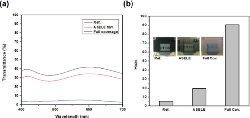
Figure 3(a) shows the measured direct transmittances (DTs). DTs were measured under air reference. In the measurements, ASELE or full coverage films were attached on the external glass surface of the encapsulated TOLEDs. Glass encapsulation caused approximately a 10% decrease in the DT [29–31]. The reference device was a TOLED with auxiliary metal buses. The DT values of the reference TOLED, ASELE TOLED and full coverage TOLED were 38%, 32% and 5%, respectively, at 550nm. The DT values of reference and ASELE film attached samples oscillates within a values of 5%. The DT of the fully covered TOLED did not exceed 5.4% in visible range. In external light extraction, the emission surface is usually covered with a light out-coupling film. Because such film is equipped with optical structures, the DT inevitably decreases by the presence of the wrinkle film, which significantly alter the optical path of the incident light. As can be seen, the average DT value of TOLED with fully covered wrinkle film is lower than 5% throughout the whole visible range. However, with the ASELE film, the decrease in the DT is only 6%. This feature allows the transparent quality of the TOLED not to be significantly reduced. Figure 3(b) shows the haze values. The haze values of the reference TOLED, ASELE TOLED and fully covered TOLED were 5.4, 20, and 91, respectively. The inset shows actual images of the aforementioned samples. While the fully covered sample shows significant blurring of the letters ETRI, no significant blurring can be observed in the ASELE TOLED. The high haze values of the fully covered TOLED strongly demonstrate the light path deflection capacity of the wrinkle structure. The increase in haze of the sample with ASELE film indicates the possibility of light extraction.
Fig. 3. The measured (a) transmittance and (b) haze values. Inset shows actual sample photographs.
Figure 4 shows the normal incidence current density(J) – applied voltage(V) –luminance (L) characteristics of bottom and top emissions. As expected, the presence of films on the external glass surface did not alter the J-V characteristics. The overall L levels of bottom emission were higher than those of the top emission. The difference in L is due to the asymmetric internal optics of TOLED. The L increased with the attachment of films, both in bottom and top emissions. The increase was higher in the bottom emission than the top emission. The results shown in Figs. 3 and 4 suggest the possibility of enhancing the efficiency of both emission sides by using ASELE films without degrading the overall transmittance of large area TOLEDs.
Fig. 4. Current density versus voltage (J-V) and voltage versus luminance (V-L) characteristics of (a) bottom emission and (b) top emission.
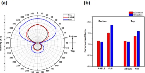
Figures 5(a) and 5(b) show the luminance distributions of bottom and top emissions as a function of viewing angle. Also, actual bottom emissions are shown [Fig. 5(c)]. The luminance distributions were obtained at a constant current density of 3 mA/cm2. The
luminance level of the bottom emission was much stronger than its counterpart, which is mainly due to the optical function of CL. To be specific the CL thickness was adjusted to enhance reflection toward the bottom, contributing to the luminance of the bottom emission. The bottom emission was almost Lambertian [Fig. 5(a)]. The top emission had stronger emission toward the viewing angle range of 30°~70°. The difference in the luminance distribution is due to the asymmetric internal optics. Attaching ASEL film yielded luminance distributions in which emissions slightly favored higher angles. The light extraction of the ASELE film was observed to be better in the bottom emission. Significant out coupling was achieved by fully covering the external glass surface with wrinkles. Figure 5(c) captures the
actual emission images. The usefulness of ASELE film can be clearly observed. The results of Fig. 5 demonstrate that by applying metal mesh aligned ASELE films, it is possible to extract more light from both emission directions without sacrificing the overall transmittance to a significant measure. In the bottom and top emission cases, these features are attributed to the wrinkle’s capacity of deflecting the light traveling path and back scattering, respectively. In particular, the widened angular luminance distribution is useful in OLED lighting.
Fig. 5. The luminance distributions of (a) bottom emission and (b) top emission. (c) Actual images of bottom emission at 0.5 mA/cm2 (upper row) and 3 mA/cm2 (lower row).
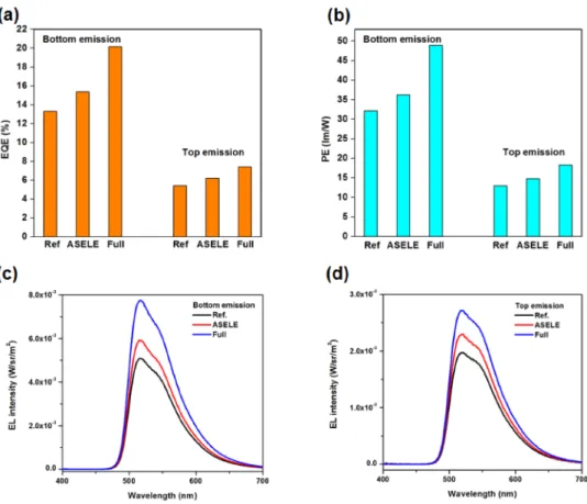
The measured external quantum efficiency (EQE), power efficacy (PE) values, and electroluminescence (EL) spectra are shown in Fig. 6. All measurements were performed using an integrating sphere. In accordance with the luminance distributions of Fig. 5, the efficiencies of the bottom and top emission were enhanced with ASELE film. In both sides increments of 15% were achieved in EQE. In the TOLEDs with the ASELE film, the bottom/top ratios of EQE and PE were 2.49 and 2.44, respectively. The main peak positions in EL spectra did not change with the application of the ASELE film or full cover wrinkle film. Technically, this feature is important because the original EL spectrum is not distorted due to the presence of ASELE film. The full width at half maximum values of the top emission EL spectra are slightly wider than their counter parts. This is thought to be an effect of differences in the internal cavity lengths. The results of Fig. 6 demonstrate the usefulness of ASELE film, which can enhance the efficiencies in both emission directions without distorting the original EL spectra.
Fig. 6. (a) The EQE and (b) PE values. The EL spectra of (c) bottom and (d) top emissions.
To elucidate the experimental results and verify the optical functions of ASELE film, optical simulations were carried out using LightToolsTM (Synopsys), a commercial illumination-optic simulation software based on ray-tracing and Monte-Carlo methods [32]. Figure 7(a) illustrates the optical simulation used in this work. With the feature size of the wrinkle on the order of 3 μm scale, the effect of the wrinkle based ASELE film was studied in the ray-optic domain [33]. PET and glass substrates have very similar refractive indices, the whole combination was treated as a single homogeneous medium with the refractive index of 1.52. The organic stack was also regarded as a single medium with the refractive index of 1.8, for simplicity. The refractive index of ITO was set at 1.8 with the extinction coefficient of 0.0035. The reflectance (Rtop), transmittance (Ttop), and absorption (Atop) of the cathode/
capping layer assembly were fixed at 35%, 32%, and 33%, respectively, which were obtained for normal incidence with thin-film optic calculation by treating the bilayer structure as a single equivalent surface under the so-called Smith’s approach [34]. For simplicity, these values were assumed to be angle-independent. To reflect the topological shapes of wrinkles in the ASELE film in simulations. To reflect the topological shapes of wrinkles in the ASELE film in simulations, a three-dimensional atomic force microscope (AFM) image of the film with a 40 × 40 μm2 scope area was imported into LightToolsTM using SolidWorksTM (Dassault Systèmes). Thicknesses and sizes of simulation structures follow the actual values of a real device. To reproduce the light source of OLED, we used an emitting layer which is composed of randomly distributed radiating point sources. The light source within the emitting layer was assumed to be a point source with isotropic emission pattern. Simulations were performed for a reference structure, a structure with the ASELE film, and a structure with a wrinkled film that fully covers the glass substrate. The thicknesses and sizes of the simulation structures were based on the actual values of a real device. Three simulations
corresponding to reference structure, structure with ASELE film, and structure with fully covered wrinkle on glass were performed.
Fig. 7. (a) Schematic diagram of optical simulation. (Ray-tracing and statistical method. The structure is not drawn in scale.) Visualizations of outcoupling enhancement mechanism due to a wrinkle film. Rays lying in the TIR angular range are only shown. (b) The Reference TOLED (No film), (c) ASELE film applied TOLED (d) full coverage of wrinkle film (red lines: wrinkle structure, not drawn to scale but magnified for visualization purpose.)
Figure 8 shows the simulated luminance distributions and increments in efficiencies. The simulated angular intensity distributions [Fig. 8(a)] of bottom and top emission reproduce the overall trend of the experimental distribution. The Lambertian distribution changes towards super-Lambertian distribution with side-emission enhanced for both bottom and top emissions. The out coupling enhancement ratios obtained from simulations also agree relatively well with the overall experimental trends [Fig. 8(b)], although there is some discrepancy in the exact enhancement ratios, which may be due to the ray-optic-based simplifications made in the simulation. In spite of this simplification, our simulations clearly demonstrate the function and effect of the proposed ASELE film on angular intensity distributions and efficiency enhancement. The method used here should thus be able to serve as a useful guideline for designing large area TOLEDs. For example, the optimal dimension of the wrinkle structure of an ASELE film could be predicted where transmittance and efficiency are well balanced.
Fig. 8. (a) Simulated intensity angular distributions. (b) Enhancement ratios of outcoupling efficiencies from experimental and simulation data.
4. Summary
To address the preservation of overall transmittance and efficiency enhancement of large area TOLEDs, we proposed and demonstrated a wrinkle based ASELE film as a technical solution. In order not to cover the open area of the substrate, the spontaneously formed wrinkle structures of the ASELS film were aligned to the auxiliary metal buses. By using the ASELE films, both in bottom and top emissions, the luminance distributions widened and the efficiencies increased without significant loss of transmittance. Optical simulations showed that the light out coupling of ASELE film in bottom and top emissions were mainly due to the lowered incident angle of light impinging on the substrate/air interface and backscattering effect, respectively. We believe that our approach can be extended to various large area light source applications in which transmittance, efficiency and angular luminance distribution matter.
Acknowledgments
This work was supported by research program “Technology Development of Low cost Flexible Lighting Surface”, which is a part of the R&D program of Electronics and Telecommunications Research Institute (ETRI).