www.advmat.de
Liquid-Flowing Graphene Chip-Based High-Resolution
Electron Microscopy
Kunmo Koo, Jungjae Park, Sanghyeon Ji, Saltanat Toleukhanova, and Jong Min Yuk*
Dr. K. Koo, J. Park, S. Ji, S. Toleukhanova, Prof. J. M. Yuk Department of Materials Science and Engineering
Korea Advanced Institute of Science and Technology (KAIST) 291 Daehak-ro, Yuseong-gu, Daejeon 34141, Republic of Korea E-mail: jongmin.yuk@kaist.ac.kr
The ORCID identification number(s) for the author(s) of this article can be found under https://doi.org/10.1002/adma.202005468.
DOI: 10.1002/adma.202005468
prolonged TEM observation. Additionally, graphene inherently has a high electrical and thermal conductivity, as well as radical scavenging properties,[20] and thus GLCs
alleviate charging,[21] heating, and
radia-tion damage to the sample under the elec-tron beam.[22,23]
However, GLCs have pocket- or well-type cells hermetically sealed by Van der Waals interactions of graphene sheets. This fully confined structure has limited their application to electron-beam-induced processes, such as mineral precipita-tion,[24] growth and etching of colloidal
particles,[4,11,25] and chemical lithiation
of electrode materials.[26] The external
stimuli required to mimic realistic reac-tions, such as reactive liquid injection, heating, and biasing current or voltage, could be implemented by the development of a graphene-based environmental cell system.[27] A transitional-type
graphene-based flow cell has recently been implemented to enhance the spatial resolution by replacing the single-side of SiNx window
at the monolithic channel-type SiNx liquid cell.[28]
Neverthe-less, the versatile structures are still required to improve the imaging performance and extend to Operando imaging with the adoption of external stimuli.
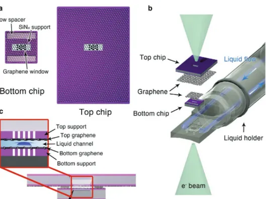
Here, we systematically designed graphene-windowed envi-ronmental cells capable of thin liquid layer formation and liquid injection (Figure 1). The liquid-flowing graphene chips (LFGCs) consist of a large top chip and a small bottom chip that fit into a commercial liquid-flowing TEM holder (Figure 1a). Each chip is fabricated by microelectromechanical system (MEMS) process on a 4-inch Si wafer, including depositing an SiNx membrane,
perforating the membrane with a holey pattern, and transfer-ring few-layered graphene onto the holey-patterned SiNx
mem-brane (Figures S1–S5 and Section S1, Supporting Information). The thick SiNx membrane and graphene serve as a
bulging-resistive support and viewing window, respectively. The fab-ricated top and bottom chips can be assembled in the liquid-flowing TEM holder equipped with a liquid injection system (Figure 1b), where liquid flows through a channel opened by spacers on the bottom chip (Figure 1c). We demonstrate the physical properties of the implemented LFGCs under harsh conditions to confirm their structural stability during LP-TEM experiments. Furthermore, using liquid-flowing graphene chip TEM (LFGC-TEM), an enhanced contrast and resolution limit were obtained with several wet samples, such as polystyrene (PS) beads, liposomes, Escherichia coli bacteria, and colloidal gold nanoparticles (Au NPs), under liquid flowing conditions.
The recent advances in liquid-phase transmission electron microscopy represent tremendous potential in many different fields and exciting new opportunities. However, achieving both high-resolution imaging and oper-ando capabilities remain a significant challenge. This work suggests a novel in situ imaging platform of liquid-flowing graphene chip TEM (LFGC-TEM) equipped with graphene viewing windows and a liquid exchange system. The LFGCs are robust under high-pressure gradients and rapid liquid circulation in ranges covering the experimental conditions accessible with conventional thick SiNx chips. LFGC-TEM provides atomic resolution for colloidal
nanopar-ticles and molecular-level information limits for unstained wet biomolecules and cells that are comparable to the resolutions achievable with solid-phase and cryogenic TEM, respectively. This imaging platform can provide an opportunity for live imaging of biological phenomena that is not yet achieved using any current methods.
Liquid-phase transmission electron microscopy (LP-TEM) has emerged as a promising platform[1–4] to directly reveal a wide
range of physical,[5–7] chemical,[8–11] and biological[12,13]
pheno-mena that take place in liquids on the nanoscale. LP-TEM requires environmental cells containing a hermetically sealed reservoir and a viewing window fabricated from SiNx.[3,8,9]
Although such liquid cells can stably maintain intact liquid samples under high-vacuum TEM conditions, both the spatial information and signal-to-noise ratio (SNR) for TEM imaging are degraded by the relatively thick (15 to 50 nm) and high-atomic-number (Z) windows.[14,15] Moreover, bulging of the
win-dows leads to a thicker liquid layer than initially intended.[16]
As an alternative window, graphene, a single-layer sheet of carbon atoms (Z = 6), has been proposed.[4,7,17] Since
gra-phene has an intrinsically high Young’s modulus (≈1 TPa), membrane bulging could be suppressed,[18] allowing for the
maintenance of a thin liquid layer within graphene liquid cells (GLCs). As a result, GLCs have provided atomic resolution and high contrast for a broad range of materials, including light elements and organic molecules. Moreover, due to the imper-meability of graphene to most molecules,[19] any aqueous or
www.advmat.de www.advancedsciencenews.com
For the rational design of the LFGC system, variables that affect the overall spatial resolution in LP-TEM were analyzed. The spatial resolution (dTEM) of LP-TEM is determined by the
Scherzer resolution (dsch), chromatic aberration-limited
reso-lution (dcc), electron dose-limited resolution (dSNR_phase), and
beam blur effect (dblur):[14]
TEM= 2sch+ 2CC+ SNR_phase2 + 2blur
d d d d d (1)
Unlike in solid-phase electron microscopy, the LP-TEM reso-lution is affected by inelastic information loss from the liquid medium and sealing membrane. Specifically, the thickness and composition of both the membrane and liquid degrade the energy (dcc) and angular (dblur) distribution of the electron beam
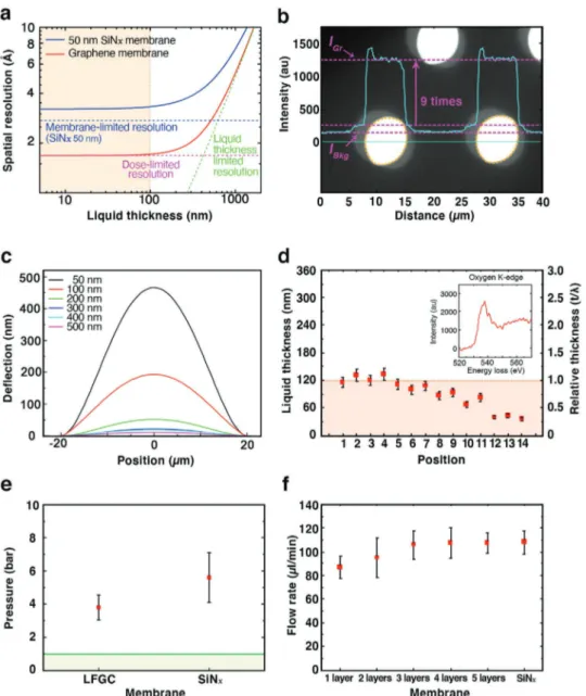
and restrict the overall resolution. Figure 2a illustrates the theoretical spatial resolution according to Equation (1) Below a liquid thickness of 100 nm, the TEM resolution is governed by membrane effects. For instance, the spatial resolution in SiNx
-based chips is restricted by the membrane-limited resolution even under the high-dose conditions applicable to the atomic-scale imaging of solid samples.[14] At the same liquid thickness,
on the other hand, the electron dose is the dominant factor for determining spatial resolution in LFGCs because graphene significantly relieves both dcc and dblur (Figure S6 and Section S2,
Supporting Information). As a result, the LFGC can provide an enhanced SNR and atomic-resolution imaging. In the assembled LFGCs, the graphene window regions have an almost 9 times higher measured brightness and more clearly resolved particle shapes than the SiNx supporting region as
proof of the relieved blur (Figure 2b and Figure S7, Supporting
Information). However, above a liquid thickness of 100 nm, the spatial resolution is determined by the liquid thickness, which hampers atomic-scale imaging regardless of the mem-brane type. Thus, a liquid thickness below 100 nm is pivotal to achieving atomic-resolution imaging in LFGC-TEM.
The liquid thickness in an environmental cell is the sum of the spacer thickness and membrane-bulged thickness. The amount of bulge is determined by both the pressure difference between the inside and outside of the liquid cells and the stiff-ness of the membrane. One approach to controlling the deflec-tion of the membrane is adjusting the internal pressure.[15]
However, this requires complex methods that are incompatible with a continuous liquid flow configuration. Alternatively, the membrane deflection can be easily controlled by geometrical approaches, either by reducing the membrane width or by increasing its thickness. However, decreasing the membrane width leads to small viewing areas, leaving thickening of the membrane as an effective way to control the bulging. Thus, membrane deflection is calculated in terms of the membrane thickness. The calculated results show that a 50 nm thick SiNx membrane has a maximum deflection of 467 nm under
a 6000 Pa pressure gradient, which is equivalent to 5 µL min−1
of liquid flow (Figure 2c and Sections S3 and S4, Supporting Information). The deflection greatly decreases to 22 nm at an SiNx thickness of 300 nm, whereas the decrement is minimized
beyond this thickness because 300 nm is the saturation point of Young’s modulus improvement of the thin film.[29] The
simula-tions showed that the deflection of the viewing window is below 26 nm with a 300 nm thick perforated support regardless of the perforation pattern (Figure S9, Supporting Information).
Figure 1. Schematics of LFGCs. a) Top view of separated LFGC. The LFGC consists of a large top chip and small bottom chip with spacers for a liquid
flow channel. At the center of each chip, perforated SiNx membranes are covered by graphene as a viewing window. b) Exploded schematic illustration of an LFGC loaded in a liquid-phase TEM holder. Liquid from outside the holder is infused through one side of the LFGC and effused to the other end. c) Cross-sectional view of an assembled LFGC. A liquid flow channel forms between the stacked top and bottom chips.
Therefore, the liquid thickness of approximately 100 nm neces-sary for atomic-resolution imaging is feasible with 30 nm thick spacers for the liquid flow channel.
The liquid thickness and internal morphology of LFGCs were calculated using electron energy loss spectroscopy (EELS) (Figure 2d and Figure S10, Supporting Information). The EEL spectra show that the liquid enclosed in LFGCs with 30 nm thick spacers has thicknesses ranging from 36 ± 3.6 to 132 ± 1.3 nm, which are in good agreement with the simulated values. Furthermore, due to the negligible inelastic scattering
from the membrane and sufficiently thin liquid layer (t/λ < 1,
where t is the sample thickness and λ is the mean free path
of the inelastic scattered electrons), it is possible to acquire a sharp oxygen core-loss edge at approximately 530 eV and ana-lyze the fine structure of oxygen in water (Figure 2d inset and Figure S11, Supporting Information).[17,30,31] Hence, the LFGCs
also benefit chemical analyses using core-loss EELS more than SiNx chips with a thick liquid layer (t/λ > 2–3).[16] Moreover, a
thin liquid layer controlled by bulging-resistive supports has the additional advantage of dissipating gas bubbles generated
Figure 2. Physical properties of designed LFGCs. a) Simulated spatial resolution of liquid cells at a dose of 1 × 10⁵ e−Å−2 including the membrane-limited
(blue dashed), liquid thickness-limited (green dashed), and electron dose-limited (magenta dashed) resolutions. Solid blue and red lines indicate the LP-TEM resolutions composed of these three factors for SiNx-based chips and LFGCs, respectively. The membrane-limited resolution in graphene is negligible. b) Electron micrograph and line profile of electron intensity showing the contrast between graphene and a 300 nm thick SiNx membrane. c) Deflection of SiNx membrane simulated with finite element analysis depending on thickness in the range from 50 to 500 nm under a 6000 Pa pres-sure gradient. d) Liquid thickness meapres-sured by the zero-loss EEL spectrum. The inset shows the oxygen core-loss spectrum meapres-sured with the LFGC. e) Pressure limit before rupture for the LFGCs and SiNx chips. The green region indicates the pressure gradient imposed on the membrane during LP-TEM experiments. f) Liquid flow rate that the LFGCs and conventional SiNx chips can withstand. The error bars in (d–f) indicate the standard deviation of 5–7 repeated experiments.
www.advmat.de www.advancedsciencenews.com
by the electron beam and retaining a constant liquid thickness because accumulated gas residues in the imaging area likely to glide freely out instead of trapping beneath deflected mem-branes (Figure S12, Supporting Information).[32]
In terms of stability during liquid cell experiments, the window must be impermeable to the solution and strong enough to prevent rupture and delamination caused by the pressure gradient and liquid stream. The impermeability of the LFGCs was examined with hydrogen gas. Hydrogen molecules were filled into the assembled LFGCs to a pres-sure of 1 bar, which was retained for more than 30 min with just one layer of graphene (Figure S13a, Supporting Informa-tion). Further, the pressure limit of the LFGCs was confirmed by a pressurized vessel test with argon gas. Based on stepwise increments in internal pressure, the LFGCs can withstand a pressure difference as high as 3–6 bar, while a 50 nm SiNx cell
can withstand 4–10 bar (Figure 2e). It was confirmed that the observed rupture initiated from the stacked graphene sheets rather than the SiNx support (Figure S13b,c and Movie S1,
Sup-porting Information). Although the maximum pressure that the graphene window can withstand is lower than that of the SiNx window due to intrinsic defects or wrinkles,[33] the
sus-pended graphene in the LFGCs is strong enough to seal liquid and gas under 1 bar, which is a commonly employed pressure for in situ liquid and gas experiments. The adhesive stability of the LFGCs against laminar force was also tested at liquid infu-sion rates from 0.1 to 120 µL min−1 (Figure 2f). A single layer
of graphene can withstand a flow rate of up to 80 µL min−1,
and graphene with more than 3 layers maintains its integrity at the maximum flow rate.
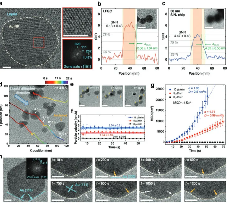
To demonstrate the enhanced imaging properties of the pro-posed systems, an Au NP dispersed solution was constantly infused into the LFGCs and analyzed. An image of the Au NPs was acquired at a high resolution of 1.47 Å, which corre-sponds to the Au {220} planes (Figure 3a). This resolving power is remarkably enhanced compared with that of previous SiNx
-based liquid cells and comparable to that of solid-phase and veil-type GLC-TEM (Figure S14, Supporting Information).[4,24]
Moreover, the LFGCs improve the SNR by ≈37% and beam blur by ≈ 52% compared with the use of 50 nm thick SiNx chips
(Figure 3b,c and Figure S15, Supporting Information).[13,15]
During the constant infusion of the solution, the liquid dif-fuses into the gaps of the LFGC,[32] triggering consistent group
movements of the NPs such as 3D displacement and rotation. The directional rolling behavior of the particles shows that their movement is affected by liquid diffusion relating with liquid infusion rate,[34] instead of stage drifts or lagging of particles by
the liquid edge (Figure 3d,e and Movie S2, Supporting Informa-tion). In a static state, a small irregular movement caused by electron irradiation was observed. In contrast, the particles col-lectively moved with constant velocities of 1.34 ± 0.16 and 2.5 ± 0.21 nm s−1 at liquid infusion rates of 5 and 10 µL min−1,
respec-tively (Figure 3f and Figure S16, Supporting Information). Additionally, the diffusivity (D) of the particles increased from 0.99 to 2.5 nm2 s−1 as the infusion rate increased. The mean
square displacement (MSD) of the particles represents super-diffusion behavior following the power law (MSD ≈ 4Dtα, α > 1,
where t is time) instead of linear diffusion, indicating Brownian motion (Figure 3g).[5–7]
Further, the corrosive etching of metal NPs was conducted by continuously flowing the etchant under a minimized electron flux. A high electron dose generates radiolysis products and accelerates the reaction kinetics to within a few minutes,[11,25]
and thus the intermediate morphology could be missed. In the LFGCs, the intermediate shape evolution of the NPs can be observed at atomic resolution during etchant flow (Figure 3h and Movie S6, Supporting Information). Etching occurs pref-erentially at the corners of the NPs, following the nearest-neighbor broken-bond model.[11] After the corners flatten and
relax to the {220} surface, dissolution occurs across the entire surface because of the similar coordination. Unlike accelerated etching by an electron beam, the repeated surface etching and flattening lead to the evolution of intermediate spherical NPs with irregular dimples, which would be missed by the electron-beam-induced etching process.
Unlike metal or inorganic nanocrystals, the mass thick-ness contrast of soft materials composed of light atoms is overwhelmed by a thick membrane and liquid.[13,21] Moreover,
improving the resolution by increasing the electron dose is restricted because soft materials are easily degraded at high elec-tron doses.[14] Therefore, the attainable resolution is limited to
up to a few nanometers under an acceptable dose of 100 e− Å−2.
Thus, to achieve high contrast and resolution with beam-sensi-tive materials, phase contrast should be employed. This phase contrast drastically decreases when the liquid becomes thicker than the single scattering mean free path of an electron, which is approximately 100–200 nm depending on the medium.[21,35]
Due to the thin liquid layer employed in the LFGCs, beam-sensitive soft materials including PS beads, liposomes, and E.
coli were directly observed without any treatments to enhance
their contrast, such as staining or tagging with metal particles. During their imaging, the PS beads and liposomes maintained their spherical shapes without degradation, and the size of the liposome lipid bilayer was discriminated as 5 nm (Figure 4a,b). Further, the rod-shaped morphology of wet E. coli bacteria and their pili with a width of 5 nm were resolved (Figure 4c,d). The 5 nm imaging resolution reaches the maximum spatial resolu-tion theoretically achievable using LFGCs at low-dose imaging conditions (Figure S6c, Supporting Information) and also cor-responds to the resolution acquired from stained samples in SiNx chips.[12]
Although the spatial resolution is restricted to a few nano-meters in a single micrograph, detailed information on molecular structures could be restored by utilizing a computational algo-rithm, such as single-particle analysis for the structural deter-mination of biomolecules. To reconstruct the structure at the molecular level, phase information should be transferred beyond the nanometer scale. Here, the phase information limit, which is the intersection of the transferred phase signal and the noise, governs the final resolution of the restored structures. To evaluate the phase information limit using the LFGCs, the contrast transfer function (CTF) of an image acquired from a 50 nm thick liquid was calculated (Figure 4e and Figure S17, Supporting Information). The cross-correlation of the acquired CTF with the simulated CTF demonstrated that the phase infor-mation is reliably transferred until 3.7 Å, where the crossover point with noise occurs (Figure 4f). This information limit is unprecedented in conventional environmental cells because the
noise from thick SiNx windows and liquid layers disrupts the
transfer of phase information on the nanometer scale. Besides, even if the liquid thickness is controllable below 100 nm, the existence of an SiNx window restricts the overall phase
infor-mation limit.[15] Moreover, this phase information limit is
com-parable to that acquired from vitreous ice by cryo-EM, which has a thickness of a few tens of nanometers.[35] This implies
that atomic-resolution structural analysis of proteins in their native environment would be feasible with LFGCs by adopting
the cryo-EM technique and a direct electron detector. Thus, LFGCs are a more appropriate liquid-cell platform for imaging soft materials at the molecular scale than conventional cells. Since the phase signal decays exponentially depending on the liquid thickness, large organisms requiring thick liquid layers should endure the loss of the phase signal, but natural contrast for specimens can be acquired without staining or tagging.[12]
In conclusion, we have presented LFGC-TEM as a novel imaging platform involving a graphene window and liquid
Figure 3. Atomic observation of Au NPs under liquid flow conditions. a) Atomic-resolution image of Au NPs suspended in a liquid environment (scale
bar, 2 nm). The maximal lattice resolution reaches 1.47 Å. b,c) Line profiles of SNR in NPs observed in an b) LFGC and c) SiNx chip. The 25–75% edge width of the maximal intensity (x25–75) shows the beam blur effect. The insets are representative electron micrographs showing the beam blur effect in
each liquid chip (scale bar, 20 nm). d) Group diffusion of NPs under continuous liquid circulation. The trajectories of particles are traced with time, and white and yellow arrows indicate moving and anchored particles on the graphene surface, respectively. e) Time-lapse images showing the particle movement of white arrows in (d) (scale bar, 20 nm). f) Velocity of particles depending on the liquid flow rate (Movies S3–S5, Supporting Information). g) MSDs of NPs at different flow rates. The dotted lines show the fitted MSDs following 4Dtα. The error bars in (f,g) indicate standard deviations of 5–10 tracked particles. h) Oxidative etching of an icosahedral Au NP by etchant flowing (scale bar, 10 nm). The inset shows how each surface is bounded at {111} plane. The yellow and white arrows indicate the positions of flattening and etching, respectively. The electron doses or fluxes for image and movie were (a) 1100 e−Å−2, (b,c) 50 e−Å−2, (d) 670 e−Å−2s, and (h) 400 e−Å−2s.
www.advmat.de www.advancedsciencenews.com
flow system. Although previous static GLCs have provided high-resolution imaging for in situ LP-TEM, their application is hampered by the low fabrication yields and small liquid volume of GLCs. The developed MEMS chips can be produced on a large scale and promote high-resolution LP-TEM experi-ments. Moreover, LFGCs can operate under more realistic conditions than small, static liquid cells, in which the compo-sition of the trapped liquid continuously changes as the reac-tion proceeds and thus may cause misleading interpretareac-tions of reaction mechanisms. Especially, flushing of generated reactive radicals and prevention of their scavenging at graphene could enable high-dose electron imaging or prolonged TEM observa-tions for biological specimens without their structural degrada-tion.[20] In addition, LFGCs offer high-contrast imaging for wet
biomolecules or cells without any markers such as tagging or staining. Thus, it is expected that single-molecule imaging for conformational dynamics, such as protein self-assembly, DNA
hybridization, and virus infection, could be studied at the mole-cular level with LFGC-TEM.
The LFGCs can be made compatible with other external stimuli systems that conventional environmental cells offer, such as a biasing voltage or current or a heating and gas envi-ronment, and thus they can be modified into various environ-mental cells such as electrochemistry graphene chips (ECGCs), liquid-heating graphene chips (LHGCs), and gas-flowing gra-phene chips (GFGCs). Furthermore, for the potential applica-tion of LFGCs to the vast area of reacapplica-tions regarding biology, energy science, and catalytic chemistry, the concept of sepa-rating the membrane and the viewing window can be modi-fied with other atomic films as needed. For example, hexagonal boron nitride instead of graphene can be used for high-temperature experiments based on its high thermal and chem-ical stability. Transition-metal dichalcogenides, such as MoS2 or
WS2, could also be used for the quantificational investigation of Figure 4. Imaging of electron-beam-sensitive materials at low electron doses. Electron micrographs of a) PS beads (scale bar, 50 nm), b) liposomes
with a lipid bilayer (scale bar, 50 nm), and c) aggregated E. coli bacteria (scale bar, 1 µm). d) Bacterial pili with a thickness of 5 nm cropped from (c) (scale bar, 50 nm). e) CTF-corrected power spectrum acquired from 50 nm thick liquid in LFGCs. f) The measured information limit is 3.7 Å, where the crossover point occurs between cross-correlation with the simulated CTF and noise signal. The electron doses for image were (a) 100, (b) 30, (c) 20, and (e) 150 e− Å−2. Used spacer in the chips were (a,b) 50 nm and (c) 200 nm.
organic compounds to avoid signal disturbance from the mem-brane elements.
Experimental Section
The detailed experimental process is available in the Supporting Information.
Supporting Information
Supporting Information is available from the Wiley Online Library or from the author.
Acknowledgements
K.K. and J.P. contributed equally to this work. This work was supported by the Samsung Research Funding & Incubation Center for Future Technology under Project Number SRFC-IT1701-15. The authors would like to thank Yun Chang Park at the National NanoFab Center (NNFC), Hye Jung Chang, Seung Min Kim, Min-Kyung Cho, and Junbeom Park at the Korea Institute of Science and Technology (KIST), and Young-Min Kim and Woo-Sung Jang at Sungkyunkwan University (SKKU) for their assistance with some of the EELS and TEM experiments.
Conflict of Interest
The authors declare no conflict of interest.
Keywords
atomic resolution imaging, biological imaging platforms, graphene liquid cells, liquid-phase transmission electron microscopy, operando electron microscopy
Received: August 12, 2020 Revised: October 24, 2020 Published online:
[1] F. M. Ross, Science 2015, 18, 350.
[2] J. J. De Yoreo, N. A. J. M. Sommerdijk, Nat. Rev. Mater. 2016, 1, 16035.
[3] N. De Jonge, F. M. Ross, Nat. Nanotechnol. 2011, 6, 695.
[4] J. M. Yuk, J. Park, P. Ercius, K. Kim, D. J. Hellebusch, M. F. Crommie, J. Y. Lee, A. Zettl, A. P. Alivisatos, Science 2012, 336, 61.
[5] H. Zheng, S. A. Claridge, A. M. Minor, A. P. Alivisatos, U. Dahmen,
Nano Lett. 2009, 9, 2460.
[6] A. Verch, M. Pfaff, N. De Jonge, Langmuir 2015, 31, 6956.
[7] Q. Chen, J. M. Smith, J. Park, K. Kim, D. Ho, H. I. Rasool, A. Zettl, A. P. Alivisatos, Nano Lett. 2013, 13, 4556.
[8] M. J. Williamson, R. M. Tromp, P. M. Vereecken, R. Hull, F. M. Ross,
Nat. Mater. 2003, 2, 532.
[9] H. Zheng, R. K. Smith, Y. W. Jun, C. Kisielowski, U. Dahmen, A. Paul Alivisatos, Science 2009, 324, 1309.
[10] J. Wu, W. Gao, H. Yang, J. M. Zuo, ACS Nano 2017, 11, 1696. [11] X. Ye, M. R. Jones, L. B. Frechette, Q. Chen, A. S. Powers, P. Ercius,
G. Dunn, G. M. Rotskoff, S. C. Nguyen, V. P. Adiga, A. Zettl, E. Rabani, P. L. Geissler, A. P. Alivisatos, Science 2016, 354, 874. [12] E. Kennedy, E. M. Nelson, T. Tanaka, J. Damiano, G. Timp, ACS
Nano 2016, 10, 2669.
[13] N. De Jonge, D. B. Peckys, G. J. Kremers, D. W. Piston, Proc. Natl.
Acad. Sci. USA 2009, 106, 2159.
[14] N. de Jonge, L. Houben, R. E. Dunin-Borkowski, F. M. Ross, Nat.
Rev. Mater. 2019, 4, 61.
[15] S. Keskin, P. Kunnas, N. De Jonge, Nano Lett. 2019, 19, 4608. [16] M. E. Holtz, Y. Yu, J. Gao, H. D. Abruña, D. A. Muller, Microsc.
Microanal. 2013, 19, 1027.
[17] C. Wang, Q. Qiao, T. Shokuhfar, R. F. Klie, Adv. Mater. 2014, 26, 3410. [18] S. P. Koenig, N. G. Boddeti, M. L. Dunn, J. S. Bunch, Nat.
Nanotechnol. 2011, 6, 543.
[19] S. Hu, M. Lozada-Hidalgo, F. C. Wang, A. Mishchenko, F. Schedin, R. R. Nair, E. W. Hill, D. W. Boukhvalov, M. I. Katsnelson, R. A. W. Dryfe, I. V. Grigorieva, H. A. Wu, A. K. Geim, Nature 2014,
516, 227.
[20] H. Cho, M. R. Jones, S. C. Nguyen, M. R. Hauwiller, A. Zettl, A. P. Alivisatos, Nano Lett. 2017, 17, 414.
[21] C. J. Russo, L. A. Passmore, Curr. Opin. Struct. Biol. 2016, 37, 81. [22] S. Keskin, N. de Jonge, Nano Lett. 2018, 18, 7435.
[23] K. Koo, K. S. Dae, Y. K. Hahn, J. M. Yuk, Nano Lett. 2020, 20, 4708. [24] J. M. Yuk, Q. Zhou, J. Chang, P. Ercius, A. P. Alivisatos, A. Zettl, ACS
Nano 2016, 10, 88.
[25] S. Y. Kim, K. S. Dae, K. Koo, D. Kim, J. Park, J. M. Yuk, Phys. Status
Solidi Appl. Mater. Sci. 2019, 216, 1800949.
[26] H. K. Seo, Y. Hwa, J. H. Chang, J. Y. Park, J. S. Lee, J. Park, E. J. Cairns, J. M. Yuk, Nano Lett. 2020, 20, 2080.
[27] F. M. Ross, Liquid Cell Electron Microscopy, Cambridge University Press, Cambridge, UK 2016.
[28] G. Dunn, V. P. Adiga, T. Pham, C. Bryant, J. Donez, J. N. Belling, B. Lafrance, J. A. Jackson, R. Barzegar, J. M. Yuk, S. Aloni, M. F. Crommie, A. Zettl, ACS Nano 2020, 14, 9637.
[29] K. B. Gavan, H. J. R. Westra, E. W. J. M. Van Der Drift, W. J. Venstra, H. S. J. Van Der Zant, Appl. Phys. Lett. 2009, 94, 233108.
[30] S. M. Ghodsi, S. Anand, R. Shahbazian-Yassar, T. Shokuhfar, C. M. Megaridis, ACS Nano 2019, 13, 4677.
[31] G. Algara-Siller, O. Lehtinen, F. C. Wang, R. R. Nair, U. Kaiser, H. A. Wu, A. K. Geim, I. V. Grigorieva, Nature 2015, 519, 443. [32] J. T. Van Omme, H. Wu, H. Sun, A. F. Beker, M. Lemang,
R. G. Spruit, S. P. Maddala, A. Rakowski, H. Friedrich, J. P. Patterson, H. H. Pérez Garza, J. Mater. Chem. C 2020, 8, 10781.
[33] L. Wang, C. M. Williams, M. S. H. Boutilier, P. R. Kidambi, R. Karnik,
Nano Lett. 2017, 17, 3081.
[34] E. A. Ring, N. De Jonge, Microsc. Microanal. 2010, 16, 622. [35] P. J. B. Koeck, A. Karshikoff, J. Microsc. 2015, 259, 197.