• 검색 결과가 없습니다.

An investigation on dicing 28-nm node Cu/low-k wafer with a Picosecond Pulse Laser

N/A
N/A
Protected

Academic year: 2021

Share "An investigation on dicing 28-nm node Cu/low-k wafer with a Picosecond Pulse Laser"

Copied!
6
0
0

로드 중.... (전체 텍스트 보기)

전체 글

(1)

An investigation on dicing 28-nm node Cu/low-k wafer with a Picosecond Pulse Laser

Hsiang-Chen Hsu

1,†

, Li-Ming Chu

2

, Baojun Liu

3

and Chih-Chiang Fu

1

1

Department of Mechanical and Automation Engineering, I-Shou University, Kaohsiung City 84001, Taiwan, R.O.C.

2

Department of Mechanical Engineering, Southern Taiwan University of Science and Technology University, Tainan City 71005, Taiwan, R.O.C.

3

Department of Mechanical Engineering, University of Electronic Science and Technology of China, Zhongshan Institute, 528402, P. R. China

(Received December 1, 2014: Corrected December 18, 2014: Accepted December 19, 2014)

Abstract: For a nanoscale Cu/low-k wafer, inter-layer dielectric (ILD) and metal layers peelings, cracks, chipping, and delamination are the most common dicing defects by traditional diamond blade saw process. Sidewall void in sawing street is one of the key factors to bring about cracks and chipping. The aim of this research is to evaluate laser grooving

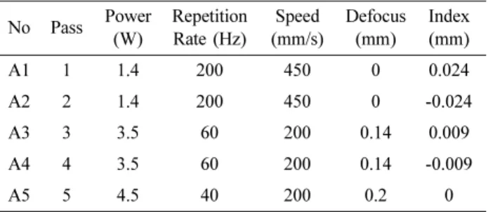
& mechanical sawing parameters to eliminate sidewall void and avoid top-side chipping as well as peeling. An ultra-fast pico-second (ps) laser is applied to groove/singulate the 28-nanometer node wafer with Cu/low-k dielectric. A series of comprehensive parametric study on the recipes of input laser power, repetition rate, grooving speed, defocus amount and street index has been conducted to improve the quality of dicing process. The effects of the laser kerf geometry, grooving edge quality and defects are evaluated by using scanning electron microscopy (SEM) and focused ion beam (FIB).

Experimental results have shown that the laser grooving technique is capable to improve the quality and yield issues on Cu/low-k wafer dicing process.

Keywords: nanoscale low-k wafer, laser kerf geometry, laser grooving

1. Introduction

As IC scales down into nanometer level, interconnect technologies on back end of the line (BEOL) are forced to move from Al/SiO

2

to Cu/low-k (Copper/low dielectric constant).

1-2)

Copper and low-k dielectric layers are implemented as multilevel interconnects to improve the speed of logic devices and reduce cross talk noise, propagation delays and power dissipation from RC delay.

Amongst the available low-k materials, black diamond (BD) has been widely used for integration in ULSI (ultra large scale integration) for its better electrical and dielectric properties.

3-4)

BD is a trade mark of Applied Materials Inc.

5)

and is silica based dielectric material, obtained by doping of silica with -CH3 groups and it has chemical formula SiOC:H. BD thin films are usually fabricated by using the chemical vapor deposition (CVD) method near room temperature. The dielectric constant (k) value of BD films ranges from 2.5 to 2.7, and integrated ILD stack dielectric constant is mostly less than 3. The glass transition temperature of the BD is well above 450

o

C. The dielectric constant of the

BD films can be lowered by introducing porosity into the microstructure in which retains thermo-mechanical properties of silicon oxide. Due to heterogeneous structure of Cu/low- k, interfacial adhesive failure may occur during fabrication processes and delamination or cracking can also be observed during packaging processes. Therefore, micromachining of nanoscale low-k wafer has been one of the crucial issues in IC packaging technology.

Laser technology has been practiced for over four decades and playing an important role in the modern manufacturing industry. Recently, high brightness of fiber/disk lasers and ultra-fast of pico-/femto-second lasers have enabled new developments in micro/nano fabrication that lasers material processing can bring to IC packaging industries. A metallized diamond saw blade has been successfully applied to separate the traditional 300 mm thickness silicon wafer.

However, damage to the silicon chips during mechanical dicing has become an extraordinary issue as nanometer node wafers with Cu/low-k dielectrics is implemented.

6-8)

Consequently, blade die saw processes confront many serious challenges, such as chipping, die breaking, cracking

Corresponding author E-mail: [email protected]

© 2014, The Korean Microelectronics and Packaging Society

This is an Open-Access article distributed under the terms of the Creative Commons Attribution Non-Commercial License(http://creativecommons.org/

licenses/by-nc/3.0) which permits unrestricted non-commercial use, distribution, and reproduction in any medium, provided the original work is

properly cited.

(2)

and delamination of the bonded layers due to the diamond- edge mechanical forces. Several new wafer-dicing techniques, such as scribe-and-break, dicing before-grinding and dicing by thinning with dry-etched trenches have been developed to overcome the above-mentioned challenges. Nevertheless, dicing using laser technology is one of the significantly efficient and improving methods.

9-10)

Laser technology works as a non-contact tool and offers a mandated micromachining process which is much more competitive than diamond blade saw. Laser process with tight focus results in diminished kerf width and reduces top-/bottom-side chipping and cracking.

Heat energy is concentrated on the laser beamed area to produce debris on the top surface of silicon wafer. Redeposition of melted silicon adheres fast to the top surface of silicon wafer and greatly damages circuits as well as reduces the performance of the IC devices. Up to present, various methods have been developed to accomplish debris-free cutting minimization of debris during wafer dicing. A soluble protective coating on the silicon wafer surface to capture the debris has become an acceptable method in the laser dicing technology. The silicon wafer is dispensed and spin-coated at first, after drying, then laser grooving is performed. A clean debris-free wafer singulation can be achieved after washing. In addition, a smooth kerf internal wall can be obtained if successive chemical wet etching is further applied.

11)

In this paper, grooving on 28-nm node Cu/low-k wafer using 10 ps pulse 512 nm wavelength laser has been conducted to determine the optimized recipes. Material in sawing street (scribe lane) comprises metal (copper), low-k (silica based dielectric materials) and protectively coated silicon. A series of experimental works has been conducted and the results can be directly applied to industrial wafer sawing process.

2. Experimental Works

The micro structure of nanoscale Cu/low-k silicon wafer used in this work includes 5 µm low-k (black diamond) ·500Å TEOS (tetraethyl orthosilicate)·250Å Ta (Tantalum)·1000Å Cu (Copper) seed·2 µm electroplating-Cu, which is shown in Figure 1.

12)

The complete wafer sawing process comprises:

laser groove and diamond blade saw. Traditional diamond blade saw process on Cu/low-k wafer (heterogeneous materials) will lead to top-/bottom-side chipping, peeling or sidewall overcutting. The void in sidewall is one of the factors to cause sidewall cracks. Therefore, laser grooving technology is introduced to nanoscale wafer dicing to

eliminate sidewall voids and improve the quality of sawing process. Water soluble coating is applied to the surface of the silicon wafer to seize the recast silicon remaining (debris). The thickness of this protective coating film is about 1 um.

The specification of ultra-fast laser machine used in this works is listed in Table 1. Parametric studies are performed based on (1) 3-pass laser grooving (2) DOE (design of experiments) using Taguchi approach (3) sidewall voids elimination in 5-pass. Parameters for standard 3-pass laser grooving, Taguchi orthogonal array and 5-pass sidewall void elimination are listed in Table 2, Table 3 and Table4, respectively.

3. Results and Discussion

Preliminary results demonstrate that parameter of power would directly affect the depth of cut, frequency results in depth of cut/surface debris, defocus relates to beam size, speed influences on surface ripple/surface debris, and index induces the overlap rate. Because the width of sawing street ranges from 65 to 70 µm, the experimental kerf width should be controlled at 45-55 µm and kerf depth is up to 35 µm. For the standard 3-pass laser grooving process, the effects of the laser kerf geometry, grooving edge quality and Fig. 1. Cu/low-k wafer micro structure.

Table 1. Specification of Laser machine used in this study.

Wavelength of laser light 512 nm

Maximum average power 30 W

Diffraction factor M

2

<1, 3

Pulse duration < 10 ps

Base frequency 200, 400, 600, 800 KHz

Maximum pulse energy 150 µJ

Beam diameter at the exit window 5 mm

(3)

defects are evaluated by 3D laser scanning microscopes and scanning electron microscopy (SEM). Figure 2 illustrates kerf geometry for 3-pass laser grooving standard recipes. The kerf depth can be controlled under 56 µm and the V-shape cut is generated under the sawing street. Figure 3(a) presents the debris on top opening and Figure 3(b) demonstrates the corresponding enlarged view of e-beam photo.

In general, DOE using Taguchi approach can economically satisfy the needs of process design optimization projects. In order to eliminate the top-/bottom side chipping and minimize the debris from heat generation Taguchi method is conducted to evaluate the optimization recipe for laser grooving. DOE parameters matrix is defined in Table 3(a) and Taguchi orthogonal array is listed in Table 3(b). The optimized recipe is found to be A1B3C3D3, i.e. 4 MHz, 15W, 600 mm/s, overlap 100% and the results is determined

in Table 4. It should be noted that all experimental data obtained in this work meet the industrial requirements.

The main advantage of using laser beam cutting is to reduce top-/bottom-side chipping and cracking. Nevertheless, most of the drawbacks of laser dicing are associated with the heat generation during laser ablation. In order to produce good quality of die sawing process, many issues need to be Fig. 2. Kerf geometry for 3-pass laser grooving scanned by Keyence 3D laser scanning microscopes (V-shape cut under scribe lane).

Fig. 3. (a) Top viewed by e-beam (b) Enlarged view of kerf width/kerf depth.

Table 2. Recipes for standard 3-pass laser grooving process.

Pass 1 Pass 2 Pass 3

Power (W) 2.8 3 2

Repetition-Rate (Hz) 160 50 40

Speed (mm/s) 300 120 300

Defocus (mm) 0 0 0

Index (mm) 47 0 0

(4)

fully understood. This includes the selection of appropriate processing parameters, analysis of metallurgical effects of

the cutting process, minimization of micro-cracks, heat affected zone, debris around the redeposit surface. Hence, an increasing in the number of passes with appropriate processing recipe would be another interesting solution for industrial process. 5-pass laser beam dicing technique then becomes alternative major fabrication process. However, the sidewall voids are sometimes produced during the third pass (pass 3) or the fourth pass (pass 4). Sidewall voids are known to be responsible for top side cracking.

Figure 4(a) schematically illustrates recipes for 5-pass laser grooving process and Figure 4(b) presents the defect of sidewall voids after sawing. The original and optimized recipes for 5-pass laser grooving are listed in Table 5(a) and 5(b), respectively. The differences between original and optimized recipes are defocus amount and controlled kerf width. Figure 5 demonstrates kerf geometry scanned by Keyence 3D microscopes for optimized recipes applied to 5-pass laser grooving process. Please be noted that U-shape cut under scribe lane can be achieved by using special- Table 3. (a) DOE parameters matrix.

Factor Level 1 Level 2 Level 3

A (Repetition

Rate) 4MHz 6MHz 8MHz

B (Power) 5W 10W 15W

C (Speed) 150 mm/s 300mm/s 600 mm/s

D (Pass &

overlap rate)

3-pass (overlap 20%)

3-pass (overlap 50%)

3-pass (overlap 100%) Table 3. (b) Taguchi orthogonal array.

No. A B C D

1 L1 L1 L1 L1

2 L1 L2 L2 L2

3 L1 L3 L3 L3

4 L2 L1 L2 L3

5 L2 L2 L3 L1

6 L2 L3 L1 L2

7 L3 L1 L3 L2

8 L3 L2 L1 L3

9 L3 L3 L2 L1

Fig. 4. (a) Schematically illustrated recipes of 5-pass Laser grooving (b) Sidewall voids generated at 3-/4-pass.

Table 4. Laser grooving results after Taguchi optimized recipes.

Item Specification Industry Standard Experimental work 1 Heat affect analysis

(Debris) < 5 µm 3.57 µm

2 Top side chipping Not allow < 0.005 µm 3 Passivation peeling Not allow < 0.005 µm 4 Laser groove depth >10 µm 15.786 µm 5 Wafer scratch Not allow <0.005 µm

6 Die crack Not allow <0.005 µm

7 Wafer broken Not allow None

8 Laser total kerf width Target ± 3 µm ± 2.73 µm

9 Laser kerf shift ± 2 µm ± 1.96 µm

Fig. 5. Kerf geometry for optimized 5-pass laser grooving by

Keyence 3D microscopes (U-shape cut under scribe lane).

(5)

designed photo mask.

Moreover, Figure 6 shows that sidewall voids has been eliminated as the laser width is constrained from 55 µm to 47 µm, i.e. kerf width for pass 1-2, pass 3-4 and pass 5 has been changed from 55, 36, 22 µm to 47, 28, 22 µm in Figure 4(a). The results also can be found in Table 6(a) and 6(b) for original and optimized recipes, respectively.

4. Conclusions

This paper demonstrates an improvement procedure for laser grooving/dicing on a nanoscale low-k wafer to eliminate the sidewall voids and top cracking. Microstructure of nanoscale wafer with Cu/low-k dielectric is presented. Due to heterogeneous materials in Cu/low-k wafer, an ultra-fast pico-second 515 nm green laser is applied to micro machine a 28 nanometer node wafer. DOE using Taguchi method has been conducted and successfully determined the standard 3- pass laser beam void-free recipes. Furthermore, parameters used to eliminate sidewall voids in 5-pass laser grooving technique are obtained. U-shape cut under sawing street has been accomplished by using a self-designed mask. All experimental data in this work satisfy the industrial requirements.

Acknowledgment

The authors would like to express their appreciation to the Ministry of Science and Technology (MOST 103-2221-E- 214-018) and the National Science Council (NSC102-2221- E-214-022) in Taiwan for financial supports.

References

1 . D. Shamiryan, T. Abell, F. Lacopi and K. Maex, “Low-k dielectric materials”, Materials Today, 7(1), 34 (2004).

2. H. H. Jiun, I. Ahmada, A. Jalarb and G. Omarc, “Effect of wafer thinning methods towards fracture strength and topog- raphy of silicon die”, Microelectronics Reliability, 46, 836 (2006).

3. S. Chen, T. Y. Kuo, H. T. Hu, J. R. Lin and S. P. Yu, “The evaluation of wafer thinning and singulating processes to enhance chip”, Proc. 55

th

Electronic Components and Tech- nology Conference (ECTC), 1526, IEEE (2005).

4. V. N. Sekhar, “Mechanical characterization of black diamond (low-k) structures for 3D integrated circuit and packaging applications”, Nanoindentation in Materials Science, 10, 229 (2012).

5. http://www.appliedmaterials.com.

6. J. Sillanpaa, J. Kangastupa, A. Salokatve and H. Asonen,

“Ultra-short pulse Laser meeting the requirements for high speed and high quality dicing of low-k wafers”, Proc.

Advanced Semiconductor Manufacturing Conference and Workshop (ASMC), Munich, 194, IEEE (2005).

7. J. V. Borkulo, P. Dijkstra and R. Hendriks, “Comparison between Single & Multi Beam Laser Grooving of Low-K lay- ers”, Proc. 45

th

International Symposium on Microelectronics (IMAPS), 433 (2012).

8. C. Paydenkar, A. Poddar, H. Chandra and S. Harada, “Wafer sawing process characterization for thin Die (75micron) appli- cations”, Proc. 29

th

International Electronics Manufacturing Technology Symposium (IEEE/CPMT/SEMI), 74, IEEE (2004).

Fig. 6. No sidewall void/no top cracking exists for optimized 5-pass laser grooving.

Table 5. (a) Original recipes for 5-pass laser grooving.

No Pass Power (W)

Repetition Rate (Hz)

Speed (mm/s)

Defocus (mm)

Index (mm)

A1 1 1.4 200 450 0 0.024

A2 2 1.4 200 450 0 -0.024

A3 3 3.5 60 200 0.14 0.009

A4 4 3.5 60 200 0.14 -0.009

A5 5 4.5 40 200 0.2 0

Table 5. (b) Optimized recipes for 5-pass laser grooving.

No Pass Power (W)

Repetition Rate (HZ)

Speed (mm/s)

Defocus (mm)

Index (mm)

B1 1 1.4 200 450 0 0.02

B2 2 1.4 200 450 0 -0.02

B3 3 3.5 60 200 0.14 0.005

B4 4 3.5 60 200 0.14 -0.005

B5 5 4.5 40 200 0.2 0

Table 6. (a) Kerf geometry for original 5-pass laser grooving.

Results

Ave. A1 A2 A3 A4 A5

Kerf Width( µm) 58 57 58 58 57 59

Kerf Depth(µm) 20 20 21 20 20 21

Table 6. (b) Kerf geometry for optimized 5-pass laser grooving.

Results

Ave. B1 B2 B3 B4 B5

Kerf Width(µm) 46 47 48 46 45 47

Kerf Depth(µm) 21 20 21 20 20 21

(6)

9. K. Shimizu, K. Takahashi, H. Morikazu, N. Ogoshi, K.

Takeyama, Y. Wakayama and T. Obara, “Laser ablation of sil- icon wafer with a water microdrop”, J. Laser Applications, 18(2), 127 (2006).

10. L. T. Beng, C. L. W. Yew, K. W. Shi, S. C. Teck and K.Y.

Yow, “Laser Grooving Process Development for Low-k Ultra Low-k Devices”, Proc. 33

rd

International Electronic Manufac- turing Technology Symposium (IEMT), Penang, 1, IEEE/

CPMT (2008).

11. H. Y. Zheng, X. C. Wang and Z. K. Wang, “Laser dicing of silicon and electronics substrates”, Advances in Laser Mate- rials Processing: Technology, Research and Application, 88 (2010).

12. H. C. Hsu and S. J. Wu, “Laser Drilling and Thermal Stress

Analysis on TSV in 3D IC Structure”, Proc. International

Conference on Electron Devices and Solid-State Circuits, 112,

IEEE (2014).

수치

Table 1. Specification of Laser machine used in this study.
Fig. 3. (a) Top viewed by e-beam (b) Enlarged view of kerf width/kerf depth.
Fig. 5. Kerf geometry for optimized 5-pass laser grooving by Keyence 3D microscopes (U-shape cut under scribe lane).
Fig. 6. No sidewall void/no top cracking exists for optimized 5-pass laser grooving.

참조

관련 문서

In particular, the dependences of maximum temperature increase and decay time constant on the laser pulse width, beam diameter, and absorption coefficient

In this study, we investigated the effects of low-power CO 2 laser on proliferation on human gingival fibroblast cells so that determine laser

A) Clinical view of the recession defects B) Tunnel preparation with VISTA C) Deepithelialization using a high-speed handpiece at the hard palate. D)

Effects of pulse frequency of low-level laser thrapy (LLLT)on bone nodule formation in rat calvarial cells.. Low-level laser therapy stimulats

SLS(Selective Laser Sintering) SHS(Selective Heat Sintering) SLM(Selective LAser Melting) EMB(Electron Beam Melting) DMD(Diret Metal Deposition). &lt;그림

SLS(Selective Laser Sintering) SHS(Selective Heat Sintering) SLM(Selective LAser Melting) EMB(Electron Beam Melting) DMD(Diret Metal Deposition). &lt;그림

Summerscales, &#34;An investigation into the effects of fabric architecture on the processing and properties of fibre reinforced composites produced by resin

This study has the following academic suggestions: First, this study focused on the effects of workplace innovation on living quality of rural people with