[논 문] 한국재료학회지 DOI: 10.3740/MRSK.2008.18.2.061 Kor. J. Mater. Res.
Vol. 18, No. 2 (2008)
61
†
Corresponding author
E-Mail : [email protected] (S. Y. Choi)
Phase Change Characteristics of Sb-Based Phase Change Materials
Sung-Jin Park, In Soo Kim, Sang-Kyun Kim and Se-Young Choi
†School of Materials Science & Engineering, Yonsei University, 134 Shinchon-Dong, Seoul 120-749, Korea (Received November 13, 2007 : Accepted December 20, 2007)
Abstract Electrical ·optical switching and structural transformation of Ge
15Sb
85, Sb
65Se
35and N2.0 sccm doped Sb
83Si
17were studied to investigate the phase change characteristics for PRAM application. Sb-based materials were deposited by a RF magnetron co-sputtering system and the phase change characteristics were analyzed using an X-ray diffractometer (XRD), a static tester and a four-point probe. Doping Ge, Se or Si atoms reinforced the amorphous stability of the Sb-based materials, which affected the switching characteristics. The crystallization temperature of the Sb-based materials increased as the concentration of the Ge, Se or Si increased. The minimum time of Ge
15Sb
85, Sb
65Se
35and N2.0 sccm doped Sb
83Si
17for crystallization was 120, 50 and 90 ns at 12 mW, respectively. Sb
65Se
35was crystallized at 170
oC. In addition, the difference in the sheet resistances between amorphous and crystalline states was higher than 10
4Ω/γ.
Key words phase change materials, Sb-based materials, PRAM .
1. Introduction
Phase change materials, namely chalcogenides, show different properties at amorphous and crystalline states.
These materials are applied to optical mass storage and phase-change random access memory (PRAM) by using their changes in optical and electrical properties upon phase transformation .
1-3)PRAM is one of the most promising candidates for the next generation nonvolatile memory devices. However, it still requires advanced materials, which exhibit low-power consumption, rapid phase transition and cyclic reliability. Recently, Sb-based materials have caught attention for the rapid crystallization behavior of Sb .
3-6)However, rapid crystallization would impede the stability of amorphous phase with unintended crystallization of amorphous recording. Thus, the main concern is to optimize the trade off condition between rapid crystallization and amorphous stability .
8-10)In this study, the main focus is on amorphizability, as a parameter to control the crystalli- zation tendency, and Ge, Se or Si was employed as an amorphous stabilizer in Sb-based materials.
2. Experimental procedure
The films were deposited by radio frequency magnetron sputtering system (SNTek, Korea) on Si (100) wafers and
slide glasses by using Ge (99.99%, RND KOREA, Korea), Se (99.997%, RND KOREA, Korea), Si (99.999%, RND KOREA, Korea) and Sb (99.999%, Kurt J. Lesker, U.S.A) targets. The base pressure was 5 ×10
−7Torr and working pressure was adjusted to 1 mTorr by introducing Ar at a rate of 10 standard cubic centimeters per minute (6N, Seoul gas, Korea) through mass flow controller. Targets were pre-sputtered for 5 minutes in order to remove oxidized surface and contaminations. Substrate holder was rotated at 20 rpm to obtain uniform thickness and homogenized composition of the films. Film composition was controlled by inducing different RF power to each target.
As-deposited films were annealed in Ar atmosphere for 10 min at 100~300
oC with a heating rate of 5 K/min. The crystal structure was analyzed by X-ray diffractometer (Rigaku D/MAX II A, Japan & Philips X'pert MRD, Philips, Netherlands). The phase transition behavior on a nano- second scale was observed by laser irradiation using static tester (PST-1, Nanostorage, KOREA). Thickness of all films was 100 nm.
3. Result and discussion
3.1 Sheet resistance
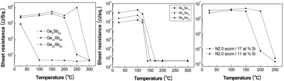
Fig. 1 presents changes in the sheet resistances of Sb-
based materials with different doping concentrations and
annealing temperatures. At room temperature, all Sb-
based materials were amorphous. The electrical switching
of Sb-based materials was confirmed from phase transition.
62 Sung-Jin Park, In Soo Kim, Sang-Kyun Kim and Se-Young Choi
In the case of Sb-Se alloys, large resistance margin between amorphous and crystalline states was observed. Especially, Sb
65Se
35has the largest value of difference. The sheet resistance was 98 M Ω/□ at room temperature and decreased to 480 Ω/□ at 170
oC. Such a decrease can be explained by the structural transformation of Sb
65Se
35. The sheet resistance of N2.0 sccm doped Sb-Si alloys at room temperature was about 5 M Ω/□. It decreased to 2 KΩ/□
after crystallization. In the case of 11at.% Si doped alloy, decrease in the sheet resistance occurred between 150
oC and 250
oC due to structural transformation. On the other hand, decrease in the sheet resistance of 17at.% Si doped alloy occurred between 200
oC and 250
oC. As the amount of Si increased, phase transition temperature increased and phase stability was also improved. In Ge-Sb alloys, difference in the sheet resistance varies with the doping concentration of Ge. As doping concentration of Ge increased, phase transition temperature increased. In addition, the margin of resistance between amorphous and crystalline states was increased. In PRAM, low phase transition temperature of phase change material may provoke unwanted phase transformation through thermal energy produced by the device operation. Therefore, phase transition temperature of around 200
oC is suitable for PRAM application. For this reason, Ge
15Sb
85, Sb
65Se
35and N2.0 sccm doped Sb
83Si
17were chosen for our experiments.
3.2 Crystal structure
Fig. 2 shows XRD patterns of Sb and Sb-based materials with different doping concentrations and annealing tem- peratures. As-deposited Sb was crystalline and had hexagonal structure. XRD pattern of Sb annealed at 300
oC exhibited Sb and Sb
2O
3phases. As-deposited Sb-based materials are at amorphous states. Thus, it is possible to deduce that Ge, Se and Si might have reinforced the amorphous stability of Sb-based materials. Ge
15Sb
85and N2.0 sccm doped
Sb
83Si
17were crystallized with heat treatment and have similar crystal structures with pure Sb. In the case of Sb
65Se
35, the 1
stphase transition was observed at 170
oC and the 2
ndphase transition was observed at 280
oC. At 280
oC, the peaks can be identified as a mixture of Sb, Sb
2O
3and Sb
2Se
3.
3.3 Crystallization behavior
To investigate the crystallization behavior in the scale of nano-seconds, static tester was employed. Fig. 3 indicates PTE (Power-Time-Effect)
6)diagram of Sb-based materials with changes in reflectivity. The reflectivity change, optical contrast ( △‚R) is defined by the following equation: △‚
R = (R
after-R
before)/R
before, where R
beforeand R
afterindicate the reflectivity before and after irradiation, respectively.
The magnitude of R is illustrated by different colors in the PTE diagram. At low laser power and/or short pulse width (1
stblue region), reflectivity does not change. When laser power and/or pulse width are increased, crystallization occurs. However, extremely high laser power and/or long pulsed width results in re-amorphization or ablation of the phase change materials (2
ndblue region). An ablation is a kind of thermal destruction. In the case of Sb
65Se
35, relatively fast and easy crystallization occurred with short pulse width and/or low laser power. However, N2.0 sccm doped Sb
83Si
17was hard to crystallize. Even at high laser power and long pulse width, ablation did not occur. It means that N2.0 sccm doped Sb
83Si
17has a good thermal stability.
Ge
15Sb
85was very difficult to crystallize, while Ge
6Sb
94was easy to crystallize (not presented). Thus, high content of Ge impedes easy crystallization, which corresponds well with the result of changes in sheet resistance at different annealing temperatures.
Fig. 4 presents a nano-second scale crystallization
behavior of Ge
15Sb
85, Sb
75Se
25and N2.0 sccm doped
Sb
83Si
17at 6, 12, and 18 mW, respectively. Reflectivity
Fig. 1. Sheet resistance change of Sb-based materials with different doping concentrations and annealing temperatures.
phase change characteristics of Sb based phase change materials 63
changed due to crystallization and ablation. In the case of Ge
15Sb
85, at 6 mW, the minimum time for crystallization
was 280 ns and ablation did not occur. At 12 mW, crystalli- zation started from 120 ns and ablation was observed at Fig. 2. XRD patterns of (a) Sb, (b) Ge
15Sb
85, (c) Sb
65Se
35and (d) N2.0 sccm doped Sb
83Si
17annealed at different temperatures .
Fig. 3. PTE(Power-Time-Effect) diagram of (a) Ge
15Sb
85, (b) Sb
65Se
35and (c) N2.0 sccm doped Sb
83Si
17with reflectivity changes .
Fig. 4. Nano-second scale crystallization behavior of Ge
15Sb
85, Sb
65Se
35and N2.0 sccm doped Sb
83Si
17with different laser power
and pulse width .
64 Sung-Jin Park, In Soo Kim, Sang-Kyun Kim and Se-Young Choi