한국표면공학회지 J. Korean Inst. Surf. Eng.
Vol. 51, No. 4, 2018.
https://doi.org/10.5695/JKISE.2018.51.4.231
<연구논문>
ISSN 1225-8024(Print) ISSN 2288-8403(Online)
P-type Electrical Characteristics of the Amorphous La
2NiO
4+δThin Films
Dang-Hoang Hop
a,b, Jung-A Lee
a, Young-Woo Heo
a, Jeong-Joo Kim
a, and Joon-Hyung Lee
a,*aSchool of Materials Science and Engineering, Kyungpook National University, Daegu 41566, Korea
bMinistry of Science and Technology of Vietnam, 113 Tran Duy Hung street, Cau Giay district, Ha Noi, Vietnam
(Received 3 July, 2018 ; revised 31 August, 2018 ; accepted 31 August, 2018)
Abstract
We report p-type electrical characteristics of the amorphous La2NiO4+δ thin films which were sputtered on the glass substrates using an RF sputtering system. As-deposited thin films at room temperature and 300oC were amorphous in nature. Post-annealing of the thin film samples over 400oC resulted in the nano-crys- tallization of the La2NiO4+δ. The electrical properties of the films were much dependent on the oxygen partial pressure, temperature of the post-annealing and sputtering ambient. The as-deposited samples at room tem- perature show a hole concentration of 7.82×1013cm-3, and it could be increased as high as 3.51×1022cm-3 when the films were post-annealed in an oxygen atmosphere at 500oC. Such p-type conductivity behavior of the La2NiO4+δ films suggests that the amorphous and nano-crystallized La2NiO4+δ films have potential for the application as p-type semiconductive or conductive materials at low temperatures where material diffusion is limited.
Keywords : Lanthanum nickel oxide, thin film, amorphous, RF magnetron sputtering, p-type
1. Introduction
Lanthanum nickel oxide (La2NiO4) is the first member of the Ruddlesden Popper (RP) family, which have the general formula Lan+1NinO3n+1 (n=1, 2, 3, ), where n is the number of LaNiO3 perovskite layers separated by LaO rocksalt-like layers stacking along the c-axis [1,2]. It is well known that La2NiO4+δ exhibits a wide range of oxygen nonstoichiometry [3], high oxygen diffusivity and surface exchange coefficients at intermediate temperatures [4]. Therefore, these properties make La2NiO4+δ promising candidate material as cathodes for intermediate temperature solid oxide fuel cells (IT-SOFCs) and for solid oxide electrolysis cells (SOECs), electrical contacts, and catalytic purposes.
On the other hand, because of the high solubility of
excess oxygen in the crystal [5], La2NiO4+d possesses p-type electrical conductivity [6,7]. Owing to the mixed ionic and electronic conductivity [5,8,9], La2NiO4+δ has been reported to be used as ionic conducting materials for SOFC with the electrical conductivity of 42.5Ω-1cm-1 at room temperature [10]
and 76Ω-1cm-1 at 800oC [4].
The transport mechanism of transparent conducting amorphous oxides with high mobility which are composed of heavy metal cations with an electronic configuration (n-l)d10nso (n>4) has been studied by Honsono et al.[11]. They explained that the large overlap between the nso orbitals which primarily constitute the bottom part of the conduction band and the insensitivity of the overlap to an angular variation is the major origin of large mobility even in amorphous stage [11]. Nevertheless, there have been no reports on the La2NiO4+δ amorphous or nanocrystalline La2NiO4+δ thin filmsas well as their applications using their p-type electronic conductivity at diffusion-limited low temperatures.
In this study, La2NiO4+δ thin films, which are a
∞
*
Corresponding Author: Joon-Hyung LeeSchool of Materials Science and Engineering, Kyungpook National University, Daegu 41566, Korea
Tel: +82-53-950-7512 ; Fax: +82-53-950-5645 E-mail: [email protected]
followed by post-annealing in oxygen in relation to the oxygen nonstoichiometric of La2NiO4+δ. Furthermore, La2NiO4+δ films were also grown in different Ar/O2 ratios at 300oC to bring out the role of oxygen nonstoichiometry (δ) in electrical properties of the La2NiO4+δ thin films.
2. Experimental
A stoichiometric La2NiO4 target with a diameter of 50 mm was fabricated by general solid state reaction and sintering process. Raw materials of NiO (99.99%, Junsei Chemical) and La2O3 (99.99%, Alfa Aesar) were used. After weighing the raw materials, the powders were wet-ball milled with zirconia balls and ethyl alcohol for 24 h. After drying, the mixture was cold isostatically pressed at 200 MPa. Sintering was conducted at 1350 oC for 2 h in the air with a heating rate of 5oC/min and then furnace cooled.
Thin films of the La2NiO4+δ were deposited on the glass substrates by using RF magnetron sputtering.
The substrate of the soda-lime glass was cleaned in TCE (Trichloroethylene), acetone and ethyl alcohol in a sequence by an ultrasonic cleaner, then dried with nitrogen gas. Prior to the deposition, the chamber was evacuated to a background pressure of 1.0×10⁻⁶ Torr initially, and both the working pressure and the RF power were fixed to 10 mTorr and 70 W, respectively. The films were deposited at room temperature for 30 minutes with an Ar/O2 ratio of 32/8 and post-annealed at different temperatures for 1 h in air. In addition, the effect of Ar/O2 ratios on the electrical characteristics of the nonstoichiometric La2NiO4+δ films were examined when the films are deposited at 300oC.
Thin film thickness was determined by the Dktak XT Stylus Profiler (Bruker) using a step method which allows high accuracy measurement. X-ray diffraction with nickel-filtered Cu-Ka radiation (X'Pert PRO, PANalytical) was used for phase identification of the thin films. Field Emission Transmission Electron Microscopy (Titan G2 ChemSTEM CS probe) also used to analyze the microstructure of the films. Electrical characteristics of the samples were analyzed using a Hall-effect measurement system (Ecopia, HMS-3000) with a constant magnetic field of 1 T at room temperature.
The optical band gap of the thin films was
determined using a UV/VIS/NIR spectrophotometer (Philips, CARY 5G).
3. Results and Discussion
The influence of post-annealing temperature on the crystallization of the La2NiO4+δ thin films was studied by X-ray diffraction as shown in Fig. 1. The as- deposited film at room temperature and the post- annealed films up to 300oC were amorphous. By further increasing the post-annealing temperature, the films began to crystallize at 400oC appearing (200) peak of La2NiO4+δ at . The broad and low intensity of the (200) peak in the post-annealed samples signifies that the films are not fully crystallized. The crystallization temperatures of the La2NiO4+δ thin films reported by P. Briois et al.and Marie-Laure Fontaine et al. were around 800~900oC which are much higher than that of this study [12,13].
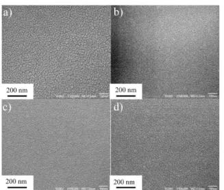
Fig. 2 (a-d) show the SEM images of the La2NiO4+δ thin films deposited at room temperature and post-annealed at 300oC, 400oC, and 500oC for 1 h in sequence. All of the thin films revealed relatively smooth surfaces. However, the surface roughness showed a decreasing tendency as the annealing temperature increased. Even though the AFM images are not presented, the annealed samples showed smoother surfaces than the pristine sample which seems to be caused by a thermally activated mass transport.
High resolution TEM investigations on the thin 2θ 33≈ o
Fig. 1. X-ray diffraction patterns of the La2NiO4+d thin films annealed at different temperatures in oxygen ambient.
films were performed to analyze the crystallization of the thin films. Fig. 3 show the TEM images of La2NiO4+δ thin films which were deposited for 30 minutes in a mixed gas of Ar/O2 with a ratio 32/8 at (a) 300oC and (b) post-annealed at 500oC for 1 h.
The selected area electron diffraction (SAED) patterns of the respective films are shown in the inset of the TEM images. The low magnification of the whole thin film image was not presented here and the thickness of the films was about 40 nm.
In the case of the Fig. 3 (a), neither clear lattice images nor sharp diffraction rings were observed, indicating that the sample is amorphous. However, the sample deposited at room temperature and post- annealed at 500oC was mostly amorphous but lattice fringes of nanometer-sized La2NiO4+δ solid grains are shown in Fig. 3 (b). The lattice fringes of the few nanometer-sized crystallites within the amorphous films show no special orientation of growth, which is
indicated by arrows. Its SAED revealed several spots indicating the existence of nanocrystallites.
Fig. 4 shows the resistivity, carrier concentration and Hall mobility of the La2NiO4+δ thin films which were deposited at room temperature and post- annealed in O2 for 5 h at different temperatures. As the annealing temperature increased from room temperature to 200oC, the resistivity decreased from 882.80Ω.cm to 47.35 Ω.cm. Since then, there has been a slight rising of resistivity to 75.20Ω.cm at 400oC. When the annealing temperature increased from 400oC to 500oC, a sudden decrease in the resistivity (4.60×10⁻⁴Ωcm) was observed. Concerning the TEM image of Fig. 3 (b), fairly large amount of crystallization might proceed in the film when it was annealed at 500oC for 5h.
Stoichiometric La2NiO4 is an electrical insulator, with Ni having a valance of +2 [14,15]. Under the common preparation conditions, however, excess oxygen (δ) is always found in La2NiO4+δ, which results in a p-type semiconductive material [16-18].
It has been reported that fairly large amounts of Ni3+
ions (2-12 wt%) are contained in La2NiO4, depending on whether the samples are prepared in air or oxygen, or whether they are polycrystalline ceramics or single crystals [19-21]. From this point of view, the decrease in the resistivity in Fig. 4 might be due to the formation of O2- interstitial introduced by post- annealing in oxygen [22,23], which leads to the hole doping by the partial valence change from Ni2+ to Ni3+ [23].
As the annealing temperature increased from room temperature to 500oC, the carrier concentration (p) increased and reached to a maximum value at 500oC.
Fig. 2. The X-ray s diffraction patterns of the La2NiO4+δ thin films deposited at a) room temperature and post- annealed at b) 300oC, c) 400oC, and d) 500oC for 1 h.
Fig. 3. TEM images of La2NiO4+δ thin films deposited at a) 300oC in a Ar/O2 ratio of 32/8 and b) post- annealed at 500oC. The inset shows the selected area electron diffraction (SAED) of the samples.
Fig. 4. Electrical resistivity (■ ), carrier concentration (▲ ), and Hall mobility ( ● ) of the La2NiO4+δ thin films deposited at room temperature and annealed at different temperatures from 200 to 500oC for 5 h in O2.
However, the mobility (μ) decreased with an increase in the annealing temperature. Generally, carrier mobility decreases with increasing concentration due to carrier-carrier scattering in semiconductor materials. On the other hand, however, decreased mobility in La2NiO4+δ was explained by the increased carrier concentration as well as ionized impurity (oxygen interstitial) scattering [18]. In this experiment of the La2NiO4+δ thin films, it is thought that the increased p dominates over the deceased µ, which consequently resulted in the decrease in resistivity.
In order to examine the effect of the oxygen interstitial (d) on the p-type conductivity of the La2NiO4+δ, the deposited films were annealed in N2, Air and O2 environments at 500oC for 5 h. The electrical resistivity, carrier concentration, and Hall mobility of the films are listed in Table 1. Thin film annealed in the O2-rich environment revealed a higher carrier concentration. This result can be explained by the fact that the post-annealing in the O2-rich environment introduced interstitial O2−, and played a role of hole doping in the films.
Fig. 5 shows X-ray diffraction patterns of the thin
films as a function of the Ar/O2 ratios which was varied from 32/0 to 32/32 during the sputtering process at 300oC. All the films are amorphous in nature regardless of the Ar/O2 ratios.
Fig. 6 shows the resistivity, carrier concentration and mobility of the films grown at 300oC in different Ar/O2 ratios. Note that all of the samples are amorphous as seen in Fig. 5. It was found that the resistivity of the La2NiO4+δ thin films decreased from 7880 to 0.18Ωcm when the Ar/O2 ratio changed from 32/0 to 32/24, i.e., oxygen partial pressure increased. At the same time, the carrier concentration increased drastically from 4.17×10¹² to 3.10×1019cm-3. The predominant defects in crystallized La2NiO4+δ are interstitial oxygen and electronic holes. In this case, the carrier concentration is closely related to the (cm-3) (cm/V·s) (Ω·cm)
N2 4.91×10¹⁸ 3.77×101 3.37×10⁻² Air 1.93×10²² 3.68×10⁻¹ 8.78×10⁻⁴ O2 3.51×10²² 3.99×10⁻¹ 4.60×10⁻⁴
Fig. 5. X-ray diffraction patterns of the La2NiO4+δ thin films deposited at 300oC in different Ar/O2 ratios.
Fig. 6. Electrical resistivity (■ ), carrier concentration (▲ ), and Hall mobility ( ● ) of the La2NiO4+δ thin films deposited at 300oC as a function of oxygen partial pressure during the sputtering process.
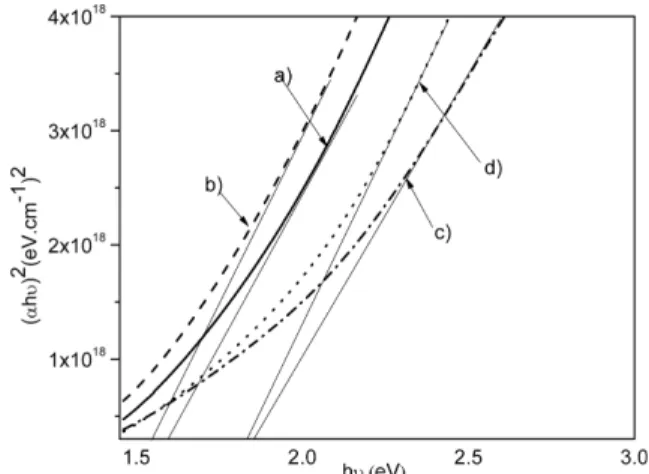
Fig. 7. Plots of (αhν)2 versus photon energy of the La2NiO4+δ thin films: a) as deposited at room temperature; b) post-annealed at 200oC, c) post- annealed at 300oC, d) post-annealed at 400oC.
number of oxygen interstitials in the lattice which in turn affect the conductivity of the crystalline La2NiO4+δ [24]. However, the increased carrier concentration in the amorphous thin films in Fig. 6 might not be adequately explained by the oxygen interstitial model. On the other hand, our previous study on the effect of oxygen plasma treatment on the electrical characteristics of the amorphous La2NiO4 thin films revealed an increase in carrier concentration after the treatment. On the basis of the XPS spectra analysis, the binding energies of oxygen and nickel ions were found to shift towards higher energies, indicating an increase in the oxidation states of the cations [25]. Therefore, although the mechanism cannot be explained exactly, annealing of the amorphous thin films in oxygen-rich ambient contributed to the increase in carrier concentration.
Stoichiometric La2NiO4 is a charge-transfer insulator with the intrinsic electrical band gap of about 4 eV [26,27]. However, Tajima et al. reported an onset of absorption at about 1.50-2 eV through optical spectrum measurements [28]. In this work, the optical energy bandgaps (as shown in Fig. 6) of the films deposited at room temperature and post- annealed at 200oC, 300oC, and 400oC were 1.60, 1.55, 1.85 and 1.84 eV, respectively.
4. Conclusions
The structural and electrical properties of the La2NiO4+δ films deposited at room temperature using RF magnetron sputtering and followed by a post- annealing treatment were investigated. The films were amorphous until they underwent the post- annealing process over 400oC. The post-annealing treatment at 500oC in oxygen atmosphere for 5 h led to a great decrease in resistivity (4.6×10⁻⁴Ω·cm). The electrical properties of the La2NiO4+δ thin films deposited at 300oC with difference Ar/O2 indicated that thin film growing in oxygen-rich ambient could lower their resistivity promptly even though the films are in the amorphous state. The results show that the post-annealing or thin film growing in an oxygen-rich environment could introduce more holes into the thin films through the oxidation of the Ni ion, thereby increasing the carrier concentration in the films.
Acknowledgment
This research was supported by Kyungpook National University Research Fund, 2015
References
[1] Sihyuk Choi, Seonyoung Yoo, Jee-Young Shin, Guntae Kim, “High Performance SOFC Cathode Prepared by Infiltration of Lan+1NinO3n+1(n = 1, 2, and 3) in Porous YSZ,” J. Electrochem. Soc., 158 [8], (2011) B995-B999.
[2] Xiaole Weng, Paul Boldrin, Isaac Abrahams, Stephen J. Skinner, Suela Kellici, Jawwad A. Darr,
“Direct syntheses of Lan+1NinO3n+1 phases (n=1, 2, 3 and ∞) from nanosized co-crystallites,” J. Solid State Chem., 181, (2008) 1123–1132.
[3] K. Ishikawa, W. Shibata, K. Watanabe, T. Isonaga, M. Hashimoto, Y. Suzuki, “Metal–Semiconductor Transition of La2NiO4+δ,” J. Solid State Chem., 131, (1997) 275-281.
[4] Duan-ping Huang, Qing Xu, Feng Zhang, Wen Chen, Han-xing Liu, Jian Zhou, “Synthesis and electrical conductivity of La2NiO4+δ derived from a polyaminocarboxylate complex precursor,” Mater.
Lett., 60, (2006) 1892–1895.
[5] R. Sayers, M. Rieu, P. Lenormand, F. Ansart, J.A.
Kilner, S.J. Skinner, “Development of lanthanum nickelate as a cathode for use in intermediate temperature solid oxide fuel cells,” Solid State Ionics, 192, (2011) 531-534.
[6] S.-Y. Jeon, M.-B. Choi, J.-H. Hwang, E. D.
Wachsman, S.-J. Song, “Electrical Conductivity and Thermoelectric Power of La2NiO4+δ,” J.
Electrochem. Soc., 158 [5], (2011) B476-B480.
[7] Mónica Burriel, José Santiso, Marta D. Rossell, Gustaaf Van Tendeloo, Albert Figueras, Gemma Garcia, “Enhancing Total Conductivity of La2NiO4+δ Epitaxial Thin Films by Reducing Thickness,” J. Phys. Chem. C, 112, (2008) 10982–
10987.
[8] V. Faucheux, M. Audier, S. Pignard, “Physical properties of epitaxial La2NiO4+δ thin films,” Appl.
Surf. Sci., 252, (2006) 5504-5507.
[9] Gemma Garcia, Mónica Burriel, Nikolaos Bonanos, José Santiso, “Electrical Conductivity and Oxygen Exchange Kinetics of La2NiO4+δ Thin Films Grown by Chemical Vapor Deposition,” J. Electrochem.
Soc., 155 [3], (2008) P28-P32.
[10] Ting Liu, Yebin Xu, Yang Li, Zhaohui Wang, Jingyuan Zhao, “Synthesis of La2NiO4 via a PVA- based route,” Ceram. Int., 37, (2011) 3361–3364.
[11] Hideo Hosono, Masahiro Yasukawa, Hiroshi Kawazoe, “Novel oxide amorphous semiconductors: transparent conducting amorphous oxides,” J. Non-Cryst. Solids, 203, (1996) 334-344.
[12] P. Briois, F. Perry, A. Billard, “Structural and electrical characterization of lanthanum nickelate
and characterization of La2NiO4+δ powders and thin films via a modified sol–gel process,” J. Solid State Chem., 177, (2004) 1471–1479.
[14] P. Kuiper, J.van Elp, G.A. Sawatzky, A. Fujimori, S. Hosoya, D.M. de Leeuw, “Unoccupied density of stages of La2-xSrxNiO4+δ studied by polarization- dependent x-ray absorption spectroscopy and bremsstrahlung isochromat spectroscopy,” Phys.
Rev. B, 44 [9], (1991) 4570-4575.
[15] G. Blumberg, M. V. Klein, S-W. Cheong, “Charge and Spin Dynamics of an Ordered Stripe Phase in Investigated by Raman Spectroscopy,”
Phys. Rev. Lett., 80 [3], (1998) 564-567.
[16] M. Sayer and P. Odier, “Electrical Properties and Stoichiometry in La2NiO4,” J. Solid State Chem., 67, (1987) 26-36.
[17] V. Faucheux, M. Audier, S. Pignard, “Physical properties of epitaxial La2NiO4+δ thin films,” Appl.
Surf. Sci., 252, (2006) 5504-5507.
[18] Mónica Burriel, Gemma Garcia, Marta D. Rossell, Albert Figueras, Gustaaf Van Tendeloo, José Santiso, “Enhanced High-Temperature Electronic Transport Properties in Nanostructured Epitaxial Thin Films of the Lan+1NinO3n+1 Ruddlesden-Popper Series (n = 1, 2, 3, ),” Chem. Mater., 19, (2007) 4056-4062.
[19] Gopalakrishnan, G. Colsmann, B. Reuter, “Studies on the La2-xSrxNiO4 (0≤ x ≤ 1) System,” J. Solid State Chem., 22, (1997) 145-149.
[20] D. J. Buttrey, H. R. Harrison, J. M. Honig, R.
R. Schartman, “Crystal Growth of Ln2NiO4 (Ln
= La, Pr, Nd) by Skull Melting,” J. Solid State Chem., 54, (1984) 407-413.
[21] C. N. R. Rao, D. J. Buttrey, N. Otsuka, P. Ganguly, H. R. Harrison, C. J. Sandberg, J. M. Honig,
“Crystal Structure and Semiconductor-Metal Transition of the Quasi-Two-Dimensional Transition Metal Oxide, La2NiO4,” J. Solid State Chem., 51, (1984) 266-269.
[23] Masashi Hasegawa, Wen-Jye Jang, Humihiko Takei, “Magnetic states of tetragonal La2NiO4+δ (δ
= 0.156, 0.181, 0.186) single crystals with excess oxygen in peroxide form,” Physica B, 226, (1996) 375-380.
[24] Seonyoung Yoo, Sihyuk Choi, Jeeyoung Shin, Meilin Liuc, Guntae Kim, “Electrical properties, thermodynamic behavior, and defect analysis of Lan+1NinO3n+1+δ infiltrated into YSZ scaffolds as cathodes for intermediate-temperature SOFCs,”
RSC Adv., 2, (2012) 4648-4655.
[25] Dang-Hoang Hop, Young-Woo Heo, Jeong-Joo Kim, Soo-Young Park, Inn-Kyu Kang, Young-Kyoo Kim, Joon-Hyung Lee, “Effect of oxygen plasma treatment on p-type electrical properties of amorphous La2NiO4+δ thin films,” Journal of Nanoelectronics and Optoelectronics. 10 (4), (2014) 475-479.
[26] H. Eisaki, S. Uchida, T. Mizokawa, H. Namatame, A. Fujimori, J. van Elp, P. Kuiper, G. A. Sawatzky, S. Hosoya, H. Katayama-Yoshida, “Electronic structure of La2-xSrxNiO4 studied by photoemission and inverse-photoemission spectroscopy,” Phys.
Rev. B, 45 [21], (1992) 12513-12521.
[27] T. Ido, K. Magoshi, H. Eisaki, and S. Uchida,
“Optical study of the La2-xSrxNiO4 system: Effect of hole doping on the electronic structure of the NiO2 plane,” Phys. Rev. B, 44 [21], (1991) 12094- 12097.
[28] S. Tajima, H. Ishii, T. Nakahashi, T, Takagi, S.
Uchida, M. Seki, S. Suga, Y. Hidaka, M. Suzuki, T. Murakami, K. Oka, H. Unoki, “Extensive study of the optical spectra for high temperature superconducting oxides and their related materials from the infrared to the vacuum ultraviolet energy region,” J. Opt. Soc. Am. B, 6, (1989) 475-482.
La12
3---Sr1 3---NiO4
∞