논문 2012-49-10-18
코오스와 파인 조정을 위한 다이나믹 주파수 스케일링 기법을 사용하는 CMOS 듀티 사이클 보정 회로
( A CMOS Duty Cycle Corrector Using Dynamic Frequency Scaling for Coarse and Fine Tuning Adjustment )
한 상 우*, 김 종 선***
( Sangwoo Han and Jongsun Kim )
Abstract
This paper presents a mixed-mode CMOS duty-cycle corrector (DCC) circuit that has a dynamic frequency scaling (DFS) counter and coarse and fine tuning adjustments. A higher duty-cycle correction accuracy and smaller jitter have been achieved by utilizing the DFS counter that reduces the bit-switching glitch effect of a digital to analog converter (DAC). The proposed circuit has been designed using a 0.18-㎛ CMOS process. The measured duty cycle error is less than ±1.1% for a wide input duty-cycle range of 25-75% over a wide freqeuncy range of 0.5-1.5 GHz.
요 약
본 논문에서는 다이나믹 주파수 스케일링 (DFS) 카운터를 사용하여 코오스, 파인 조정 기능을 갖는 CMOS 듀티 사이클 보 정회로를 제시한다. DFS 카운터는 디지털-아날로그 컨버터의 비트 스위칭 글리치를 감소시키기 때문에 제안하는 CMOS 듀티 사이클 보정회로의 듀티 보정 범위를 증가시키고 지터 특성을 개선한다. 제안하는 회로는 0.18-㎛ CMOS 공정을 이용하여 설 계되었다. 0.5-1.5GHz의 넓은 동작 주파수와 25-75%의 넓은 듀티 사이클 보정 범위 내에서 측정된 최대 출력 듀티 사이클 에 러는 ±1.1%이다.
Keywords: Clock duty cycle, duty cycle corrector, DCC, DLL
* 학생회원, 홍익대학교 전자정보통신공학과
(Department of Electronic and Electrical Engineering, Hongik University)
** 정회원-교신저자, 홍익대학교 전자전기공학부
(Department of Electronic and Electrical Engineering, Hongik University)
※ This work was partly supported by the IT R&D program of MKE/KEIT (No. 10039159) and Business for Cooperative R&D between Industry, Academy and Research Institute funded Korea Small and medium Business Administration (No.
000419970110). The chip fabrication was supported by IDEC.
접수일자:2012년5월23일, 수정완료일:2012년9월17일
Ⅰ. Introduction
Most clock driven integrated digital systems such as memories and processors use both the rising and falling edges of a clock signal to achieve high-speed operation. Therefore, timing and synchronization circuits such as delay-locked loops (DLLs) and phase-locked loops (PLLs) usually consist of a duty-cycle correction (DCC) circuit capable of
correcting a clock with an arbitrary duty-cycle to a 50% duty-cycle clock. DCCs can be classified into three categories: analog[1], digital[2], and hybrid[3]. Analog DCCs are usually implemented by using a simple negative feedback loop and show better accuracy and a wide duty correction range but are unable to support low-power standby or power-down mode operations. In analog DCCs, standby power is consumed because the analog change pump should be turned on to keep the DCC locking information.
Unlike analog DCCs, digital DCCs[2~3] can be turned off during standby mode. Digital DCCs, however, usually have limited duty-cycle correction range, occupy a larger area, and consume more active-mode power than analog DCCs[4~5]. A hybrid DCC was introduced to combine the advantages of analog and digital DCCs[5]. In conventional digital and hybrid DCCs, to achieve high duty-cycle accuracy and small jitter performance, the duty-cycle locking time may be longer than that of an analog DCC to reduce the bit-switching glitch errors.
In this paper, we present a mixed-mode DCC that has a DFS counter for coarse and fine tuning adjustments. By consisting of both analog and digital feedback loops and utilizing dynamic frequency scaling, the proposed DCC can achieve small duty-cycle error and small clock jitter by minimizing the bit-switching glitch errors.
Ⅱ. Proposed mixed-mode DCC architecture and circuit design
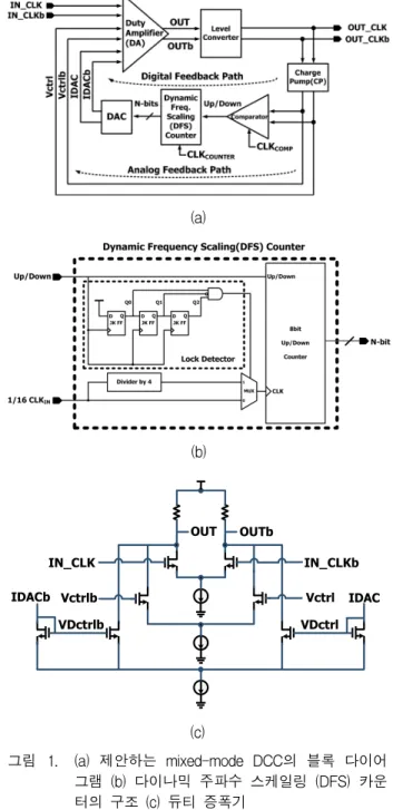
Fig. 1(a) shows the block diagram of the proposed mixed-mode DCC. It consists of a duty amplifier (DA) and a level converter in the forward path.
There are two closed loops in the feedback path: an analog feedback loop and a digital feedback loop. In the analog feedback loop, the charge pump (CP) generates the analog control voltage Vctrl/Vctrlb proportional to the clock duty-cycle of the output clock (OUT_CLK/OUT_CLKb). The Vctrl/Vctrlb
(a)
(b)
IN_CLK
Vctrlb
IN_CLKb
Vctrl OUT OUTb
IDACb IDAC
VDctrlb VDctrl
(c)
그림 1. (a) 제안하는 mixed-mode DCC의 블록 다이어 그램 (b) 다이나믹 주파수 스케일링 (DFS) 카운 터의 구조 (c) 듀티 증폭기
Fig. 1. (a) Proposed mixed-mode DCC block diagram (b) structure of the Dynamic frequency scalinig (DFS) counter (c) Duty amplifier.
voltage is also used in the digital feedback loop to generate the digital control voltage VDctrl/VDctrlb.
The digital feedback loop consists of a comparator, a dynamic frequency scaling (DFS) counter, and a simple N-bit DAC, where N=8 in this design. The comparator generates the up or down signals depending on the CP outputs. The DFS counter is a
1.0 0.8 Control Voltage
Vctrl
Vctrlb
VDctrl
VDctrlb 0.9
0nS 0.4uS 0.8uS 1.2uS T
0.7 1.1
Coarse Tune Period Fine Tune
Period
DCC locking time
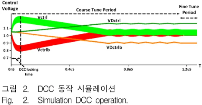
그림 2. DCC 동작 시뮬레이션 Fig. 2. Simulation DCC operation.
conventional up/down N-bit counter with variable CLKcounter operating frequency that is 1/16 (coarse tuning) or 1/64 (fine tuning) of the input clock frequency. The digital output of the DFS counter is then used for the DAC input. The DAC provides the quantized bias current IDAC/IDACb to generate VDctrl/VDctrlb. The two control voltages, Vctrl/Vctrlb and VDctrl/VDctrlb, are then used for the DA to correct the clock duty-cycle of the input clock, IN_CLK/IN_CLKb. The DA shown in Fig. 1(c) is a resistor-loaded differential pair with three input stages. The DA corrects external small-swing differential input clock signals with duty-cycle distortions. It generates a small-swing 50%
duty-cycle clock, OUT/OUTb. Finally, the level converter, which acts as a small-swing to CMOS conversion circuit, produces a full-swing output clock signal, OUT_CLK/OUT_CLKb. The digital feedback loop is positioned in parallel with the analog feedback loop to support low-power standby (or power-down) mode operation.
Fig. 2 shows the simulated operation of the proposed mixed-mode DCC. During the DCC locking time, the analog feedback loop transforms the duty-cycle error of the input clock into the analog control voltage Vctrl/Vctrlb. This analog type DA control voltage first corrects the output clock duty-cycle to 50% in a few tens of input clock cycles. The digital control voltage VDctrl/VDctrlb generated by the digital feedback loop then slowly replaces the analog control voltage during the coarse tune period with a CLKcounter operating frequency that is one-sixteenth the input clock frequency. This
means that the DFS counter has two operating frequency modes. The operating frequency of the DFS shown in Fig.1(b) can be automatically adjusted by using a lock detector which detects the up/down signal toggling between up and down sequentially. At the end of the coarse tune period, the DCC enters in to the fine tune period when the lock detector of the DFS counter is enabled by detecting Q[2:0]=[101] in Fig.1(a). Then the operating frequency of the DFS decreases to be come one-fourth of the coarse tune period frequency to achieve higher duty-cycle accuracy and lower clock jitter by decreasing the effect of bit-switching glitches. When the analog feedback loop is fully replaced by the digital feedback loop, the Vctrl and Vctrlb voltages become almost equal. The Vctrl and Vctrlb can be fully equalized to further increase the duty-cycle accuracy and decrease clock jitter by holding the DFScounter.
Ⅲ. Experimental Results
The proposed mixed-mode DCC has been fabricated and evaluated using 0.18-㎛ CMOS technology. The proposed DCC can be powered down to achieve low-power standby or power-down mode.
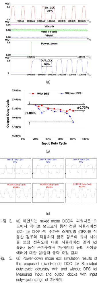
It should also have the lowest possible wakeup time in order to ensure that the 50% duty-cycle clocks at the start of the DCC. Fig. 3(a) shows the power-down exit simulation results of the proposed DCC. When Power_down is low, the DCC is powered down; when Power_down becomes high, the DCC should quickly recover. As shown in Fig. 2(a), the transition time from the power-down to active mode is about 1clock cycle; the output clock duty of 50% is maintained without distortions.
Fig. 3(b) shows the duty-cycle correcting accuracy of the proposed mixed-mode DCC with and without DFS. During the coarse tune period without DFS, the operating frequency of the DAC and the counter is 1/16 of the input clock frequency, and it shows a duty-cycle error of ±1.88% for an input duty-cycle
(a)
±0.73%
±1.88%
With DFS Without DFS
(b)
INPUT Duty-Cycle 25%
OUTPUT Duty-Cycle 49.58%
INPUT Duty-Cycle 50%
OUTPUT Duty-Cycle 49.34%
INPUT Duty-Cycle 75%
OUTPUT Duty-Cycle 50.79%
(c)
그림 3. (a) 제안하는 mixed-mode DCC의 파워다운 모 드에서 액티브 모드로의 동작 전환 시큘레이션 결과 (b) 다이나믹 주파수 스케일링 (DFS)를 적 용한 경우와 적용하지 않은 경우의 듀티 사이 클 보정 정확도에 대한 시뮬레이션 결과 (c) 1GHz 동작 주파수에서 25-75%의 듀티 사이클 에러에 대한 입/출력 클락 측정 결과
Fig. 3. (a) Power-down mode exit simulation results of the proposed mixed-mode DCC (b) Simulated duty-cycle accuracy with and without DFS (c) Measured input and output clocks with input duty-cycle range of 25-75%
range of 25-75% at 1GHz. During the fine tune period with DFS, by changing the operating frequency of the counter and the DAC to 1/64 of the input clock frequency, the duty-cycle error is decreased to ±0.73%. By utilizing DFS, the bit-switching glitch effect of the DAC is decreased and the duty-cycle correction accuracy is increased by approximately 60%. Fig. 3(c) shows measured input and output clocks at 1GHz. It achieves a measured duty-cycle error of less than ±1.1% for an input duty-cycle range of 25-75% over a frequency range of 0.5-1.5GHz.
Fig. 4 shows the chip layout and microphotograph of the proposed DCC. The mixed-mode DCC occupies an active area of 0.04mm2. It has a power dissipation of about 4.8mW for a 1.8V supply at 1GHz. Table 1 summarizes the performance comparison of the proposed mixed-modeDCC with other DCCs.
그림 4. 제안하는 mixed-mode DCC의 칩 레이아웃과 마이크로포토그래프
Fig. 4. Chip layout and chip microphotograph of the
proposed mixed-mode DCC
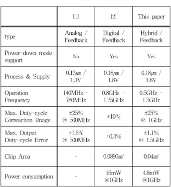
[1] [2] This paper
type Analog /
Feedback
Digital / Feedback
Hybrid / Feedback Power-down mode
support No Yes Yes
Process & Supply 0.13㎛ / 1.3V
0.18㎛ / 1.8V
0.18㎛ / 1.8V Operation
Frequency
140MHz - 780MHz
0.8GHz - 1.25GHz
0.5GHz - 1.5GHz Max. Duty-cycle
Correaction Rnage
±25%
@ 500MHz ±10% ±25%
@ 1GHz Max. Output
Duty-cycle Error
±1.6%
@ 500MHz ±0.3% ±1.1%
@ 1.5GHz
Chip Area - 0.0896㎟ 0.04㎟
Power consumption - 16mW
@1GHz
4.8mW
@1GHz
표 1. 성능 비교 표
Table 1. Performance Comparison Table.
Ⅳ. Conclusion
A mixed-mode duty-cycle corrector (DCC) circuit with coarse and fine tuning adjustments has been developed to achieve high duty-cycle accuracy and small jitter. The digital feedback loop enables the support of low-power standby and power-down modes. The DFS counter with variable operating frequency was used to reduce the bit-switching glitch effect of the DAC and achieve high duty-correction accuracy. The proposed DCC, designed and fabricated in a 0.18-㎛ 1.8-V CMOS process, occupies and active area of 0.04mm2 and dissipates 4.8mW of power .It achieves a duty cycle error of less than ±1.1% for an input duty-cycle range of 25-75% over a frequency range of 0.5-1.5GHz.
Ⅴ. Acknowledgments
This work was partly supported by the IT R&D program of MKE/KEIT (No. 10039159) and Business
for Cooperative R&D between Industry, Academy and Research Institute funded Korea Small and medium Business Administration (No. 000419970110). The chip fabrication was supported by IDEC.
참 고 문 헌
[1] B. Kim, K. Oh, L. Kim, and D. Lee ”A 500MHz DLL with Second Order Duty Cycle Corrector for Low Jitter“
IEEE Custom Integrated Circuits Conference, 2005, pp. 325-328
[2] J. C. Ha, J. H. Lim, Y. J. Kim, W. Y. Jung, J.
K. Wee, “Unified all-digital duty cycle and phase correction circuit for QDR I/O interface,”
IET Electronics Letters, 2008, pp. 1300-1301
[3] S. Han and J. Kim, “Hybrid duty-cycle correctorcircuit with dual feedback loop,” IET Electronics Letters, Vol. 47, No. 24, pp. 1311-1313, Nov., 2011
[4] S. K. Kao and S. I. Liu, “All-Digital Fast-Locked Synchronous Duty-Cycle Corrector,”
IEEE Trans. On Circuits and Systemsm, 2006,
Vol. 53, pp. 1363-1367[5] P. Chen, S. Chen, and J. Lai, “A Low power wide range duty cycle corrector based on pulse shrinking/stretching mechanism,” IEEE Asian
Solid-State Circuits Conference, 2007, pp. 460–
463
저 자 소 개 한 상 우(학생회원)
2010년 홍익대학교 전자전기 공학부 학사 졸업.
2012년 현재 홍익대학교 전자정보통신공학과 석사 졸업
2012년~현재 홍익대학교 전자 정보통신공학과 박사과정
<주관심분야 : Integrated Circuit Design, DLL/
PLL, Duty-Cycle corrector Circuit>
김 종 선(정회원)-교신저자 1992년 한양대학교 전자공학과
학사 졸업.
1994년 포항공과대학교 전자전기 공학과 석사졸업.
2006년 University of California, Los Angeles (UCLA) 전기공학과 박사 졸업.
1994년~2008년 삼성전자 메모리사업부 DRAM 설계팀 책임연구원
2008년~현재 홍익대 전자전기공학부 조교수
<주관심분야 : Analog IC design, High Speed Interface, RF Interconnect, Signaling and Clocking Circuits, Low-Power Memory Design>