항공용 레이다의 3차 고조파 믹서 설계에 대한 연구
고민호*ㆍ강세벽**
A New Third-Order Harmonic Mixer Design for Microwave Airborne Radar
Min-Ho Go*ㆍSe-Byeok Kang**
요 약
본 연구는 주파수 체배기 이론을 이용하여 초고주파 항공용 레이다를 위한 3차 고조파 믹서 설계에 대한 연구이다. 기본 믹서 설계 방법과는 달리 주파수 체배기 이론을 이용하여 국부 주파수(LO)의 3차 고조파 성분 이 최대가 되는 게이트 바이어스 전압을 선택하여 중간주파수(IF)에서 3차 고조파 혼합(mixing) 성분이 최대 가 되도록 하였다. 제안한 고조파 믹서는 플라스틱 패키지의 상용 GaAs MESFET 소자를 이용하여 설계 및 제작하여 기존 초고주파 믹서의 높은 변환손실, 회로 복잡성, 높은 가격 및 제작 복잡도를 개선할 수 있었다.
제안한 설계 방법을 이용한 3차 고조파 믹서는 33 GHz ~ 36 GHz 대역에서 8 ~10 dB 변환손실 특성 및 0 dBm 선형성 (P1dB) 특성을 나타내었다.
ABSTRACT
In this paper, a third-order harmonic mixer is designed using frequency multiplier theory for the microwave airborne radar. Unlike the basic mixer design method, the gate bias voltage, at which the third-harmonic component of the Local frequency (LO) is the maximum, is selected using a frequency multiplier theory to maximize the third-harmonic mixing component at the intermediate frequency (IF). The proposed harmonic mixer was designed and manufactured using a commercial GaAs MESFET device in a plastic package, and it was possible to improve the high conversion loss, circuit complexity, high cost, and manufacturing complexity of the existing microwave mixer. The harmonic mixer using the proposed design method has a -8 ~ -10 dB conversion loss by pumping 11.5 GHz LO with a +5 dBm level when operating from 33.0 GHz to 36.0 GHz and the 1-dB gain compression point (P1dB) of 0 dBm.
키워드
Harmonic Mixer, Multiplier, GaAs MESFET, Airborne Radar
* 한화시스템 항공레이다팀 수석연구원 ([email protected])
* 교신저자 : 한화시스템 항공레이다팀 선임연구원 ㆍ접 수 일 : 2020. 08. 17
ㆍ수정완료일 : 2020. 09. 14 ㆍ게재확정일 : 2020. 10. 15
ㆍReceived : Aug. 17, 2020, Revised : Sep. 14, 2020, Accepted : Oct. 15, 2020 ㆍCorresponding Author : Min-Ho Go
Avionics Radar Team, Hanwha Systems Email : [email protected]
Ⅰ. Introduction
Over the last ten years, there has been an unprecedented growth in the number of systems
that use the microwave and millimeter wave bands.
The design parameters, such as low cost, high performance and reproducibility, are important considerations to design in microwave and http://dx.doi.org/10.13067/JKIECS.2020.15.5.827
millimeter wave systems [1]. The SHP (Sub-Harmonically Pumped) mixer, using an anti-parallel diode, has been used in the microwave and millimeter bands because of the advantage of low LO frequency, low spurious response, and noise suppression. But many sub-harmonic mixers, with an anti-parallel diode, were used and bonded to the circuit using silver epoxy [2] or were fabricated using a MMIC realization [3] resulting in higher cost and less reproducibility. Compared with conventional mixers, with an anti-parallel diode, SHP mixers using a active device which have similar SHP mixer properties as their diode counterparts have been developed, where two active devices are pumped in anti-phase at half of the LO frequency. The active SHP mixers, with anti-phase LO input [4], have a disadvantage of larger size, higher cost, and less reproducibility in their MMIC and Hybrid realization.
In this paper, a Ka-band harmonic mixer, with a plastic packaged active device, is proposed to overcome these disadvantages of previous reported harmonic mixers. This harmonic mixer design is based on the multiplier theory that there is a bias point to maximize a specific harmonic order with respect to a fundamental LO frequency. This can get the high-order mixing element (±) to be greater than other mixing elements, pumping a RF frequency (fRF) and LO frequency (fLO), because of the bias voltage for the maximum third-order harmonic element (3fLO). The proposed harmonic mixer described in this paper offers several advantages over that of conventional SHP mixers or high-order harmonic mixers. Similar to using a commercial GaAs MESFET, it gives economical cost and good efficiency of production. In addition, the proposed mixer has an additional advantage of small size because it does not use an additional phase shift circuit. The paper is organized as follows. SectionⅡ covers the design procedure of the harmonic mixer. The fabrication and
performance of the proposed mixer and conclusion are discussed in section Ⅲ and Ⅳ.
Ⅱ. Design Method of Harmonic Mixer 2.1 Bias selection based on multiplier theory The major nonlinearity in the FET causing harmonic generation are the drain clipping, which is the most impressive effect on the harmonic generation as compared with to others’ nonlinear elements [5]. An even harmonic occurs when the output current or output voltage waveform is distorted asymmetrically. On the other hand, an odd harmonic occurs when the output waveform is distorted symmetrically to positive peak. Those effects are controlled by bias or drain termination.
The gate bias and gate input signal are selected to maximize the output level of the desired harmonic element by an approximation relating the harmonic drain current to the FET conduction angle. The harmonic drain current () can be represented as a Fourier series expansion as a function of conduction angle and can be written as Equation (1) [6].
≈max
cos
≥
≈max
(1)
Where is the drain current for the harmonic
is the average of the drain current max is the maximum drain current, and is the conduction angle. From Equation (1), Fig. 1 shows harmonic output current as a function of conduction angle.
Conduction angle should be chosen to give high in order to maximize the desired harmonic output power. The optimum conduction angle is approximately for the maximum
Fig. 1 Normalized harmonic current as a function of the conduction angle.
Biasing A-class and overdriving the FET is proper to generate at the output a signal waveform rich with the desired third harmonic as there is a clipping due to pinch-off on the negative swing and due to gate conduction on the positive swing [7]. Fig. 2 shows the output power level of a fundamental (fLO), second harmonic (2fLO) and third harmonic (3fLO) element of a local signal by adjusting gate bias voltage (Vgs) for the applied LO signal. From Fig.2, there is a specific gate bias voltage where the third harmonic is the maximum.
Fig. 2 Output harmonic generation as the gate bias 2.2 Stability design
The feedback of a fundamental element and harmonics at the drain can result in an unstable circuit [8]. The sufficient elimination of unwanted harmonics and the proper stabilization of the circuit, even if some of the conversion gain must be
sacrificed, can be adjusted to ensure stability. Fig.
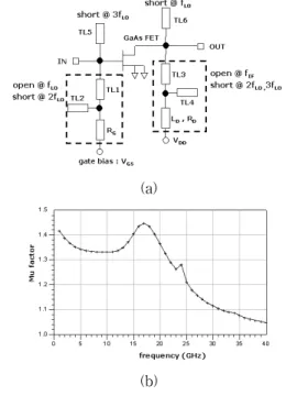
3(a) shows the circuit for stable operation with the gate bias in maximizing the third harmonic frequency as in the previous step. The gate bias network (TL1/TL2/RG) typically includes a high impedance quarter wave length line at the fundamental LO frequency (fLO). This is so that no fundamental power leaks into the DC bias and acts as a short-circuit at the second harmonic LO frequency (2fLO) as it becomes half wave length at the second harmonic (2fLO). The open stub (TL5) at the gate acts as a short-circuit at the third harmonic LO frequency (3fLO) fed from the drain port. The drain circuit (TL3/TL4/RD) also provides sufficient rejection of harmonics, and provides short-circuit terminations to harmonics at the drain to ensure stability. The open stub (TL6) at the drain acts as a short-circuit at the fundamental harmonic LO frequency. Fig. 3(b) show the circuit stability factor is greater than one over the full frequency band
(a)
(b)
Fig. 3 (a) Circuit (b) Stability factor with respect to frequency.
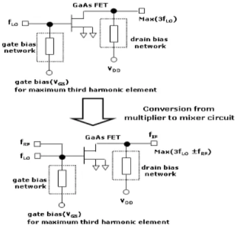
2.3 signal injection port selection for mixer Single active mixers are generally categorized into one of three topologies; gate, drain, and source mixers. In the case of the gate mixer, both LO and RF signals are applied to the gate while the IF is extracted from the drain terminal. The FET is biased near pinch-off so that the applied LO signal can modulate the transconductance of the FET over a highly nonlinear operating regime. For the drain mixer, the LO and RF signals are applied to the drain and gate, respectively, while the IF signal is extracted from the drain. This mixer operates with the FET drain-source voltage near the knee region. In a source FET mixer, the LO and RF signals are fed into source and gate respectively while the IF signal is extracted from the drain. This topology allows a modest degree of LO-to-RF isolation. Since the source FET mixer does not require a coupler or combiner, it is a simple structure compared with other mixer topologies. However, this configuration requires careful bypassing technique in the source for the IF frequency in order to suppress instability. The LO (fLO) and the RF (fRF) are inputted to the gate and the IF (fIF) is outputted to the drain as a gate mixer structure, which has higher conversion gain then other mixer topologies such as drain mixer and source mixer. Fig. 4(a) shows the conversion from the designed circuit based on multiplier theory to mixer circuit. The gate bias voltage is selected to maximize the third harmonic signal (3fLO) by the previous section.
Fig. 4 The concept of converting from multiplier to mixer circuit.
Fig. 5 shows the structure of the harmonic mixer, The LO and RF to input gate after each matching, and IF is to the drain after the low pass filter. The gate bias voltage of the proposed mixer is selected on multiplier theory to maximize the third harmonic LO signal (3fLO). The LO matching circuit is designed by a large signal scattering parameter as a large signal LO is applied. The matching circuit of the RF and IF ports is designed as quasi-linear because the RF and IF ports of impedance are affected by LO signal level [9].
Fig. 5 The proposed harmonic mixer configuration.
The gate bias voltage of the harmonic mixer is selected to make the mixing component between the applied RF signal (33.5GHz) and third harmonic signal (34.5GHz) of the pumped fundamental LO signal (11.5GHz) to be maximum, which let the
Fig. 6 shows the conversion loss characteristic of the harmonic mixer as a function of gate bias voltage. The conversion loss of the third (n=3) harmonic mixer is –10dB when the gate bias voltage (Vgs) is –0.5V for maximum third harmonic generation. On the other hand, the conversion loss of the fundamental (n=1) harmonic mixing component is –42dB by the fundamental LO signal and the conversion loss of the second (n=2) harmonic mixing component is –55dB by the second LO signal.
Fig. 6 The conversion loss of the third-order harmonic mixing and fundamental , second harmonic mixing.
Ⅲ. Experiment and Analysis
The mixer is fabricated on a Teflon substrate, which has dielectric constant 2.17, 0.5mm substrate height and 18μm conductor thickness. Fig. 7 shows the fabricated harmonic mixer. For analysis, the low pass filter and gate bias circuit are designed by Momentum Analysis. Design and optimization are performed by using the Agilent ADS (Advanced Design System) tool.
Fig. 7 Photograph of fabricated harmonic mixer
Fig. 8 shows the measurement results of conversion loss performance at the IF as a function of gate bias voltage when the fundamental LO signal is +5dBm. Conversion loss is approximately –10dB when the gate voltage is –0.5V. As seen from the result, the conversion loss is rapidly decreased at other bias points except the gate bias voltage, which makes the third harmonic LO maximum.
Fig. 8 The variation of the conversion loss with respect to gate bias voltage
Fig. 9 shows the conversion loss as a function of the LO level when the gate bias voltage is -0.5V. The conversion loss is about -10dB when LO level is from +5 dBm to +10 dBm.
Fig. 9 The conversion loss performance with respect to LO power
The output spectrum is approximately -52.5 dBm when the gate bias voltage is -0.5V with the fundamental LO level +5 dBm and RF level –40 dBm, as seen in the Fig. 10.
Ref RF
(GHz) Device Order Loss
(dB) Tech.
this 33∼36 FET 3 8 ∼10 Sodering
[4] 34∼40 PHEMT 2 9.5 MMIC
[10] 38∼38.16 PHEMT 2 15 MMIC
Fig. 10 IF output spectrum of the harmonic mixer.
Fig. 11 shows conversion loss performance as a function of RF frequency. The conversion loss is -8∼-10 dB when operating from 33.0 GHz to 36.0 GHz, which is lower than other published harmonic mixers at the Ka-band.
Fig. 11 The conversion loss with respect to RF frequency.
Fig. 12 shows the linearity performance of the harmonic mixer when changing the RF signal level (33.5 GHz). As seen from Fig. 12, the 1-dB gain compression point (P1dB) is approximately 0 dBm.
Fig. 12 1-dB compression performance.
Fig. 13 shows the isolation performance at the each port with the same environment for measuring the output spectrum. It is shown that the LO-RF isolation performance, worse than the RF-IF isolation, and the LO-IF isolation performance as known a single gate mixer’ disadvantage. Table.1 summarizes the performance of the third harmonic mixer with other referenced papers.
Fig. 13 Isolation performance.
Table 1. Performance comparisons
Ⅳ. Conclusion
In this paper, a new design method based on a frequency multiplier is proposed for a harmonic mixer. The harmonic mixer that has 8dB ∼ 10dB conversion loss by selecting the gate bias voltage which let the third harmonic component of the fundamental LO signal to be maximum is designed and fabricated. As compared with the other papers, the proposed design method for harmonic mixer has many advantages, not only in electrical performance such as low conversion loss, but also in cost and circuit complexity by using a commercial GaAs MESFET with a plastic package.
References
[1] J. Na, D. Roh and D. Kim, “Fin-Line Balanced Mixer Design for Ku-band Tracking Radar Receiver,” J. of the Korea Institute of Electronic Communication Science, vol. 13, no. 4, Aug.
2018, pp. 685-694.
[2] T. Y. Yum, Q. Xue, and C. H. Chan, “Novel
sub-Harmonically Pumped Mixer
Incorporating Dual-Band Quarter-Wave and In-Line Stub,” IEEE MTT-S Internal Microwave Symp., vol. 1, Philadelphia, USA, 2003, pp.
87-90.
[3] P. Bernkopf and Y. Tajima, “A Monolithic Ka-Band Sub-Harmonically Pumped Frequency Converter,” IEEE Microwave and millimeter-Wave Monolithic Circuits Symp., Boston, USA, 1991, pp. 43-46.
[4] K. S. Ang, A. H. Baree, S. Nam, and I. D.
Robertson, “A Millimeter-Wave Monolithic Sub-Harmonically Pumped Resistive Mixer,”
Int. Microwave Symp. vol. 2, Singapore, 1999, pp. 222-225.
[5] C. Rauscher, “High-frequency doubler operation of GaAs field effect transistors,”
IEEE Tans. Microwave Theory Tech., vol.
MTT-31, no. 6, 1983, pp. 462-473.
[6] E. O’ciardha, “Generic-device frequency multiplier analysis a unified approach,” IEEE Trans. Microwave Theory Tech., vol. MTT-48, no. 7, July 2000, pp. 1134-1141.
[7] H. Fudem and E. C. Niehenke, “Novel millimeter wave active MMIC triplers,” IEEE MTT-S Int. Microwave Symp. Digest, Vol.2, Baltimore, USA, May 1998, pp. 387-390.
[8] M. Fairburn, B. J. Minnis, and J. Neale, “A novel monolithic distributed mixer design,”
IEEE Colloquium on Microwave and Millimeter Wave Monolithic Integrated Circuits, London, UK, Nov. 1988, pp.13/1-13/6.
[8] J. Kim, I. Yoon, M. Go and H. Park, “Design and Implementation of Broadband RF
Amplifier for Microwave Receiver,” J. of the Korea Institute of Electronic Communication Science, vol. 10, no. 6, Jun. 2015, pp. 665-670.
[9] Y. H. Liew and J. Joe, “RF and IF ports Matching Circuit synthesis for a Simultaneous Conjugate-Matched Mixer Using Qualsi-Linear Analysis,” IEEE Trans. Microwave Theory and Tech., vol. 50, no. 7, Sept. 2002, pp. 2056-2062.
[10] Y. L. Kok, M. Ahma, H. Wang, B. R. Allen, and T. Lin, “A Ka-Band Monolithic Single-Chip Transceiver Using Sub-harmonic Mixer,” IEEE Radio Frequency Integrated Circuits (RFIC) Symp., Baltimore, USA, 1998, pp. 309-311.
저자 소개
고민호(Min-Ho Go) 2003년 LG이노텍 선임연구원 2010년 인하대학교 대학원 전자공 학과 졸업(공학박사)
2010년 인하대학교 차세대 항공전자통신 인력양성사 업단 연구원
2010년 ∼현재 한화시스템 수석연구원
※ 관심분야 : RFIC/MMIC, 레이다시스템
강세벽(Se-Byeok Kang) 2012년 2월 한국해양대학교 전파공 학과 졸업(공학학사)
2012년 2월 올제텍 연구원
2017년 4월 LS오토모티브 주임연구원 2019년 10월 ∼ 현재 한화시스템 선임연구원
※ 관심분야 : 레이다신호처리, 레이다시스템