486
한국표면공학회지 J. Korean Inst. Surf. Eng.
Vol. 49, No. 6, 2016.
https://doi.org/10.5695/JKISE.2016.49.6.486
<연구논문>
ISSN 1225-8024(Print) ISSN 2288-8403(Online)
Formation of One-dimensional Nb
2O
5Nanostructures by Anodization
Kiyoung Lee
*School of Nano & Materials Science and Engineering, Kyungpook National University, Sangju 37224, Korea
(Received November 22, 2016 ; revised December 5, 2016 ; accepted December 6, 2016)
Abstract
In the present work, we investigate the anodization of Nb in a K2HPO4 containing glycerol electrolyte at elevated temperatures (180oC). Under optimized conditions, uniformly over the entire anodized surface, self-organized porous Nb2O5 structures can be formed. The growth rate of highly ordered Nb2O5 is 1.7 µm/
min at beginning stage of anodization and the overall current efficiency is 70 %.
Keywords : Nb2O5, Self-organization, Porous Structure, Anodization
1. Introduction
One-dimensional metal oxide structures have led to the drastically development of nanotechnology domain for several decades. The fascinating structures exhibit novel physical properties owing to their unique geometry with high aspect ratio.
The usage is widely expanded from template for the growth of ordered arrays to direct use such as electronics, sensors, and filtration [1-4]. Many techniques have been developed to grow these one-dimensional nanostructures. Particularly, TiO2 nanotubes by anodization fluoride ion containing electrolyte are attracted many attentions and achieved various type of TiO2 nanotubes [5-7] and their novel applications [8-9]. Parallel to the success, several anodic metal and alloy oxides with wide band gaps are attracting increasing attentions [10-12].
In 1998, Melody et al. reported a novel anodization approach to grow tantalum pentoxide on tantalum
without a drop of growth rate over time (so called non-thickness-limited (NTL) growth) that can be achieved by anodization in K2HPO4 containing glycerol electrolytes at elevated temperatures (160 ~ 220oC) [13].
Recently, Anodization of Ti in K2HPO4 containing hot glycerol electrolyte were achieved. Under opti- mized conditions, the diameter and morphologies are able to control [4, 14]. By extension, highly ordered Ta2O5 nanoporous structures also can be formed by such anodization conditions [15].
Nb2O5 is highly promising materials for energy storage devices like Li insertion battery, super- capacitor [16]. Nevertheless, studies about anodic formation of Nb have been limited due to its limited thickness of anodic oxide layer [17].
In this work, we explore the feasibility to use the anodization approach to achieve highly aligned Nb2O5 nanostructures by optimizing electrolyte or electrical conditions.
2. Experimental
Niobium foils (0.125 mm thick, 99.9% purity, Advent, England) were degreased by sonication in acetone, ethanol and isopropanol, successively
*
Corresponding Author :Kiyoung LeeSchool of Nano & Materials Science and Engineering, Kyungpook National University
Tel : +82-54-530-1333 ; Fax: +82-54-530-1339 E-mail : [email protected]
Kiyoung Lee/한국표면공학회 49 (2016) 486-489 487
followed by rinsing with deionized water; finally the samples were dried with nitrogen gas.
The electrolyte for anodization was 10 wt%
K2HPO4 (Sigma-Aldrich) in anhydrous glycerol (99.8% purity, < 1% H2O, Fluka). Prior to anodiza- tion, the electrolyte was held at 200oC for 4 h to reduce the water content. For our purposes, optimized anodization conditions were found at a temperature of 180oC. Anodization was carried out in a two- electrode system configuration with a Pt foil counter electrode using a DC power supply at various voltages for various times. After the anodization process, the samples were washed in deionized water and then dried in a nitrogen stream.
For morphological characterization, a field-emission scanning electron microscope (FE-SEM, Hitachi SEM FE 4800) was used.
X-ray diffraction analysis (XRD, X’pert Philips PMD with a Panalytical X’celerator detector) using graphite monochromized CuKα radiation (Wavelength 1.54056 Å) was used for determining the crystalline structure of the samples.
3. Results and Discussion
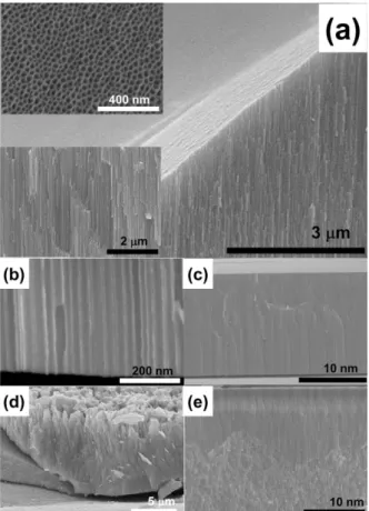
In a series of preliminary experiments, the anodiza- tion of Nb in 10 wt% K2HPO4 in glycerol electrolyte at 180oC was explored at different potential. The most promising condition to grow highly aligned Nb2O5 layers was at 7 V (Fig. 1(a) - (c)). Applied potential is highly related to morphologies and the growth rates of oxide layers. Fig. 1(a) is the 45o inclined plane views of SEM image that are obviously show highly ordered porous structures from truncated plane (upper inset) and cross-section view (lower inset and Figure (b)). The cross- sectional SEM images (Fig. 1 (b) - (c)) show highly ordered porous Nb2O5 structures formed by anodization for 3 h that are consist of approximately 78 µm of thickness with individual pore diameters of approximately 30 nm and a wall thickness of less than 10 nm (Fig. 1(b) - (c)).
The oxide layers can be formed by lower potential such as 1 V (Fig. 1(c)), but the structures consist of very small pore, irregular structures and thinner than optimized conditions. By higher potential such as 30 V, the aligned porous structures are branched
or merged (Fig. 1 (d) and (e)). The irregular parts are spread with triangular shape. In other word, to achieve highly aligned oxide layers (Fig. 1(a) and (b)), the anodization voltage is one of the critical factors.
From the result, applied potential does not only contribute to formation of oxide layer but also electrochemical dissolution of oxide layer. It is noteworthy that well aligned anodic formation of porous Nb oxide in hot glycerol electrolyte is competing reaction between oxide growth and dissolution. Moreover, ill-defined porous structures at high potential (higher than 30 V) are caused by intensive gas evolution. In principle, limited water is contained in the electrolyte due to preheating process and high temperature condition. Nevertheless, violent gas evolution occurs at such high applied potential.
Fig. 1. (a) 45o inclined view, truncated plane view (upper inset) and cross-section view (lower inset) of SEM images of highly ordered Nb2O5 structures formed at 7 V. (b)-(c) High magnified cross-sectional SEM images of (a) layer. (d) and (e) cross sectional SEM image of porous Nb2O5 formed at (d) 1 V and (e) 30 V. Porous Nb2O5 structures were formed by anodization in 10 wt % K2HPO4 contained glycerol electrolyte at 180oC.
488 Kiyoung Lee/한국표면공학회 49 (2016) 486-489
In order to in-depth study about water in electrolyte, anodization was performed without prehea- ting process (Fig. 2 (a) and (b)). The cross- sectional SEM images show that outer most part of oxide layers are intensively etched out that leads to wire like structures (7 V). When the anodization performed higher potential (20 V) in non-preheated electrolyte, the porous structures are diminished. From the results, water in electrolyte mainly plays role as etchant in the anodization system.
Figure 3 (a) shows the current density transient and the calculated charge density during anodization under optimum conditions such as anodization in preheated 10 wt% of K2HPO4/glycerol electrolytes at 7 V and 180oC. Fig. 3(b) shows that thickness of the oxide layer during anodization evolves with a similar trend as the charge. The growth rate of oxide layers is 1.7 µm/min during the first 20 min and then it is decrease to 280 nm /min. The calculated current efficiency for the formation of the oxide is approximately 70% based on Faraday’s law. The oxide was assumed to be stoichiometric niobium pentoxide and the density of anodic niobium oxide was taken as 4.74 g/cm3 [18].
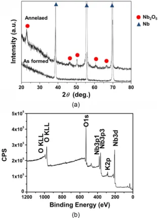
From the XRD (Fig. 4 (a)) patterns of as- formed Nb2O5 nanostructures only substrate Nb metal peaks are appeared which means that the as-formed oxide layers are amorphous phase. This result indicate that the anodic formation process following plastic flow mechanism. In order to investigate of crystal structure of the layer, oxide layers were annealed at 650oC in N2 atmosphere.
In case, the formed oxide layers were annealed in air, the substrates Nb metal also were intensively oxidize. For this reason, anodic Nb2O5 should be
Fig. 2. (a) - (b) Cross-sectional SEM images of Nb2O5 formed by anodization without preheating process at (a) 7 V and (b) 20V. The anodization was performed in 10 wt % K2HPO4 contained glycerol electrolyte at 180oC.
Fig. 3. (a) Current density transients and charge recorded during anodization at 7 V in 10 wt % K2HPO4 contained glycerol electrolyte at 180oC. (b) Influence of anodization time and charge on porous layer thickness.
Fig. 4. (a) XRD spectra of highly ordered Nb2O5 structures of layer (a) without and with annealing at 650 oC in N2. (b) XPS spectra of layer (a).
Kiyoung Lee/한국표면공학회 49 (2016) 486-489 489
annealed in inert conditions such as N2 or Ar.
The heat treated structures are fully crystallized with Nb2O5 (Fig. 4 (a)).
To investigate of stoichiometry of anodically formed Nb oxide chemical analysis were performed with XPS measurements. The XPS spectra confirm that as-formed oxide layers consist of Nb2O5 with atomic concentrations of Nb (54.6 at%) and O (17.28 at%) that were determined and the detailed spectra of the Nb3d doublet (206.6 eV) and the O1s core level (350.2 eV) [19].
4. Conclusions
We examined the formation of porous Nb2O5 structures in K2HPO4 / glycerol electrolyte at elevated temperatures. The anodic oxide structures are strongly affected by electrolyte condition (temperature and water content) and applied voltage. In the present work, we show that highly aligned porous structures with an overall pore diameter of approximately 30 nm and a thickness of several tens micrometers can be obtained under optimized anodization con- ditions with high current efficiency (70%).
Acknowledgments
This work was supported by the National Research Foundation of Korea Grant funded by the Korean Government (NRF-2016R1D1A1B03930423).
References
[1] H. Masuda, K. Fukuda, Science 268 (1995) 1466- 1468.
[2] H. Masuda, F. Hasegawa, S. Ono, J. Elecrochem.
Soc. 144 (1997) L127 – L130.
[3] C. R. Martin, Science 266 (1994) 1961-1966 [4] K. Lee, D. Kim, P. Roy, I. Paramasivam, B.I.
Birajdar, E. Spiecker, P. Schmuki, J. Am. Chem.
Soc. 132 (2010) 1478 -1479.
[5] V. Zwilling, E. Darque-Ceretti, A. Boutry-Forveille, D. David, M.Y. Perrin, M. Aucouturier, Surf.
Interface Anal. 27 (1999), 629 -637.
[6] A. Ghicov, P. Schmuki, Chem. Commun. (2009) 2791 - 2808.
[7] J. M. Macak, H. Tsuchiya, P. Schmuki, Angew.
Chem. Int. Ed. 44 (2005) 2100 -2102.
[8] K. Lee, A. Mazare, P. Schmuki, Chemical Reviews 114 (2014) 9385 - 9454.
[9] P. Roy, D. Kim, K. Lee, E. Spiecker, P. Schmuki, Nanoscale 2 (2010) 45 - 59.
[10] I. Sieber, H. Hildebrand, A. Friedrich, P. Schmuki, Electrochem. Commun. 7 (2005) 97 - 100.
[11] H. Tsuchiya, J.M. Macak, A. Ghicov, L. Taveira, P. Schmuki, Corros. Sci. 47 (2005) 3324 - 3335.
[12] W. Wei, J.M. Macak, P. Schmuki, Electrochem.
Commun. 10 (2008) 428 - 432.
[13] B. Melody, T. Kinard, P. Lessner, Electrochem.
Solid-State Lett. 1 (1998) 126-129.
[14] D. Kim, K. Lee, P. Roy, B.I. Birajdar, E. Spiecker, P. Schmuki, Angew. Chem. Int. Ed. 48 (2009) 9326 - 9329.
[15] K. Lee, P. Schmuki, Electrochem. Commun. 13 (2011) 542 – 545.
[16] X. He, J. Wu, X. Li, X. Gao, X, L. Wu, L. Zhao, X. Gan, F. Zhuge, Thin Solid Films 518 (2009) 94 - 98.
[17] J. E. Yoo, J. Choi, Electrochimica Acta, 55 (2010) 5142 - 5147.
[18] J. P. S. Pringle, Electrochim. Acta 25 (1980) 1423 – 1437.
[19] J. E. Moulder, W. F. Stickle, P. E. Sobol, K. D.
Bomben. Handbook of X-ray Photoelectron Spectroscopy, (Ed.: J. Chastain), Perkin-Elmer Corporation, Minnesota, 1992