20
A Resistance Deviation-To-Time Interval Converter Based On Dual-Slope Integration
Zhi-Heng Shang*, Won-Sup Chung*★, and Sang-Hee Son*★
Abstract
A resistance deviation-to-time interval converter based on dual-slope integration using second generation current conveyors (CCIIs) is designed for connecting resistive bridge sensors with a digital system. It consists of a differential integrator using CCIIs, a voltage comparator, and a digital control logic for controlling four analog switches. Experimental results exhibit that a conversion sensitivity amounts to 15.56 μs/Ω over the resistance deviation range of 0-200 Ω and its linearity error is less than ±0.02%. Its temperature stability is less than 220 ppm/℃ in the temperature range of -25-85℃. Power dissipation of the converter is 60.2 mW.
Key words: Resistive bridge sensor, Direct digital readout, resistance-to-time converter, second generation current conveyorm, Dual-Slope
* Dept. of Semiconductor Engineering, Cheongju University
[email protected], 043-229-8462
★ Corresponding author
※ Acknowledgment
Circuit simulation tools were supported in part by IDEC in Korea.
Manuscript received Agu 25, 2015; revised Nov 4, 2015 ; accepted Nov 5. 2015
This is an Open-Access article distributed under the terms of the Creative Commons Attribution Non-Commercial License (http://creativecommons.org/licenses/by-nc/3.0) which permits unrestricted non-commercial use, distribution, and reproduction in any medium, provided the original work is properly cited.
I. Introduction
Due to their high sensitivity, resistive sensor bridges are widely employed in industrial and process control systems and medical instrumentation. In order to interface these sensors with digital systems, an accurate interface circuit converting a small change of
resistance into a digital readout is required.
Several circuits are available in the literature for realization of such converters [1]-[7]. These are usually based on a resistance bridge. In these converters, the resistance deviation of resistive bridge sensors is converted into its corresponding offset voltage via a resistive bridge, this offset in turn is converted into a frequency (or time) by various oscillator circuits. A main drawback of these converters is that their frequency (or time period) outputs are proportional to not only the resistance deviation of sensors but also the timing component values.
The timing components usually have poor temperature stability and parasitic capacitances.
The interface circuit which is not affected by the timing components is one based on charge-balancing type A/D converters, such as sigma-delta and dual-slope converters. These circuits give their outputs a digital pulse rate or a pulse width proportional to the bridge
imbalance and synchronous with the clock frequency. The interface circuits based on a sigma-delta A/D converter have been reported [8], [9]. These circuits have the advantages of simple structure and high noise rejection.
However, they have a major disadvantage: their conversion characteristics are sensitive to temperature and supply voltage variations since their outputs are not only a function of resistance deviation but also a function of nominal resistance of sensor and current ratio of supply currents. Another disadvantage of these circuits is that the conversion resolution is limited by the delay imbalance of analog switches [8].
In this paper a new interface circuit with simple configuration and high stability on variations of temperature and nominal resistance of sensor is presented [10]. The proposed circuit is based on dual-slope integration using second generation current conveyors (CCIIs).
Ⅱ. Circuit Description and Operation
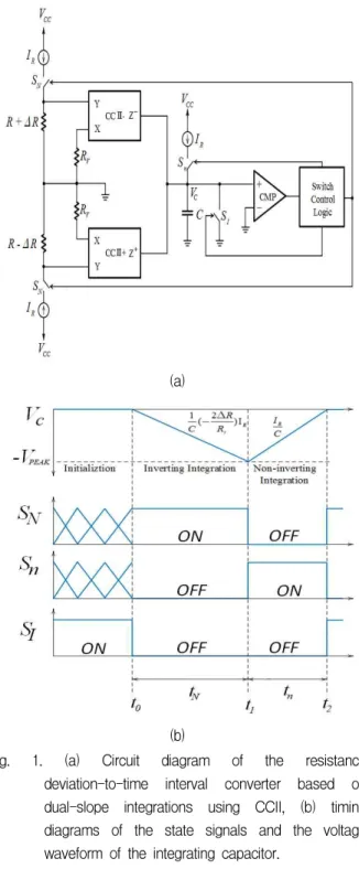
Fig. 1(a) shows the circuit diagram of the proposed resistance deviation-to-time interval (RD-to-TI) converter based on dual-slope integration. Here, resistors connected to the terminal Y of the CCIIs are half-bridge resistive sensors and connected to the terminal X is the fixed resistor. The converter consists of a differential integrator implemented with two CCIIs and a capacitor , a comparator, and digital control circuits. Symbols and circuit diagrams of the CCIIs are shown in Fig. 2 [11]. CCII+ consists of a unity-gain buffer formed by transistors - and two Wilson-current mirrors formed by -. In CCII- four Wilson-current mirrors are required.
The operation of the converter can be
divided into three states: “Initialization”,
“Inverting integration”, and “Non-inverting integration”, whose sequence and the voltage
(a)
(b)
Fig. 1. (a) Circuit diagram of the resistance deviation-to-time interval converter based on dual-slope integrations using CCII, (b) timing diagrams of the state signals and the voltage waveform of the integrating capacitor.
waveform of the integrating capacitor at each state are shown in Fig. 1(b). The detailed operation in each state will be described in the following.
(a) (b)
Fig. 2. Symbols and circuit diagrams of CCIIs used for the converter in Fig. 1: (a) CCII+; (b) CCII-.
2.1 Operation in “Initialization” state
In this state, while analog switch is kept
“on”, analog switches and do not matter.
During this state, capacitor is discharged and its voltage is kept to zero.
2.2 Operation in “Inverting Integration” state
In this state, is kept “on”, while and are kept “off”, thereby the analog circuit forms the inverting integrator, which is composed of the half-bridge resistive sensors, the reference current , the fixed resistor , the positive current conveyor CCII+, the negative current conveyor CCII-, and the capacitor . During this state, the current flowing through the capacitor is given by
∆
(1)
where ∆ is the resistance deviation of the half-bridge sensors to be detected and converted into a time interval by the converter.
This current charges the capacitor, and thus capacitor voltage may be expressed as follows:
∆
(2) where is the initial voltage of the capacitor . Equation (2) indicates that the capacitor voltage linearly ramps down with a slope of ∆. This inverting integration is carried out for a fixed period of time as shown in Fig. 1(b). Assuming that the initial voltage of the capacitor is 0 V, the accumulated voltage of the capacitor at the end of the time period is given by
∆
(3)
After this integration the converter turns into the “Non-inverting integration” state.
2.3 Operation in “Non-inverting Integration”
state
In this state, is kept “on”, while and are kept “off”, thereby the analog circuit forms the inverting integrator consisting of and capacitor . During this state, the current flowing through capacitor is
(4)
Therefore may be expressed as follows:
(5)
This shows that the capacitor voltage ramps up with a slope of until the ramp reaches back to zero as shown in Fig. 1(b). The zero crossing of the capacitor voltage will be detected by the comparator, which will then trigger digital control circuits to produce switch control signals for initializing the converter, and
the conversion cycle repeats. Let is the time duration of this non-inverting integration state, and combine (3) and (5). Then the relation between and ∆ may be expressed as follows:
∆
(6)
This equation indicates that the output time interval is directly proportional to the resistance deviation ∆. It is noticeable that the output time interval is independent of nominal resistance of sensor unlike the other works [2], [5]. This makes the converter have high stability on variations of temperature and nominal resistance of sensor. The digital values of ∆ can be known by counting the number of clock pulses gated into a counter for the time duration .
Ⅲ. Non-Ideal Effects
For the proposed RD-to-TI converter, the CCII was implemented using bipolar transistor as shown in Fig. 2. Ideally, the input resistance at the X terminal of the CCII is zero and that at the Y terminal is infinite. The output resistance at the Z terminal of the CCII is infinite.
However, the CCII actually has finite resistance for each terminal. The input resistance at the Y terminal is about 13 MΩ and that at the X terminal is about 150 Ω. The output resistance at the Z terminal is about 15 MΩ, which is sufficiently high to be negligible. Considering these finite resistances into the circuit analysis, the output of the converter can be expressed as follows:
∆
∆
(7)
where is the input resistance of the X terminal, and is the input resistance of the Y terminal. Equation (7) can be rewritten using
Taylor series expansion as
∆
∆
(8)
This result indicates that the values in round brackets of right hand side are an error produced by the non-ideal input resistances of CCIIs.
Ⅳ. Experimental Results
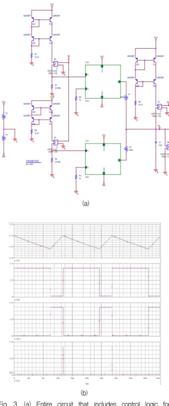
Based on the scheme in Fig. 1, a prototype circuit was built using discrete components.
Transistors arrays 2N2222 and 2N2907 were used for implementing CCIIs. The bias currents
of CCII+ and CCII- were set to 200 μA.
The comparator was LM311. All of these devices were biased with ± V. The capacitor
was 0.6 μF. A Wilson current mirror, which is formed by transistor arrays 2N2907 and resistor of 8.8 kΩ, was used to produce the reference current of 400 μA. The reference resistors were 1 kΩ. The clock frequency used in the control logic circuit was 3.3 MHz. ∆ was changed in 20 Ω steps from its fixed offset value of kΩ. Resistance was measured using Agilent digital multimeter type 34405A, and HP frequency counter 53131A was used to measure the time duration of the output pulse streams.
Fig. 3 (a) shows the entire circuit that includes control logic for experiment. Fig. 3 (b) shows the measured voltage waveforms of the circuit in fig. 3 (a).
CCII
CCII
VCCVEE
Y
X
Z VCC
VCC
VEE
VEE V2
5
V3 5
0
VC CCII-
CCII-
VCCVEE
Y
X
Z
Sn1 VCC
VEE R1
{1k+Rx}
0 R2
1k
0
R3 1k
0 R4 {1k-Rx}
0 VCC
V4 0Vdc
V5 0Vdc
C1 0.6u
0 +
- + - S2
S VON = 1.0V VOFF = 0.0V
+ - + - S3
S VON = 1.0V VOFF = 0.0V
0
0
0 + - + - S4
S VON = 1.0V VOFF = 0.0V
0 U1
LM311 OUT7 + 2
- 3
G1 8V+
V- 4
B/SB 6 5 VCC
VEE
0 0
R6 10.7k R7 10.7k
R8 10.7k SN
SI
PARAMETERS:
Rx = 160 Q19
Q2N2907
Q20 Q2N2907
+ - + - S1
S VON = 1.0V VOFF = 0.0V 0
SN Q13
Q2N2907
Q14 Q2N2907
Q21 Q2N2907
Q22 Q2N2907
0
Q23 Q2N2907
Q24 Q2N2907
Carry U15
74LS163A
CLR1
A 3
B 4
C 5 6D CLK 2
ENT 10 7ENP
LOAD 9
QA14 QB13 QC12 QD11 RCO15
SI U4A
74LS08 1 2
3
U5B
74LS08 4 5
6 VCC
Q15 Q2N2907
CLK CLK OFFTIME = 305.1757813ns ONTIME = 305.1757813ns DELAY = STARTVAL = 0 OPPVAL = 1
Q16 Q2N2907
0
VCC U11
74LS163A
CLR1
A 3
B 4
C 5 6D CLK 2
ENT 10
7ENP LOAD 9
QA14 QB13 QC12 QD11 RCO15
Carry
U12
74LS163A
CLR1
A 3
B 4
C 5 6D CLK 2
ENT 10
7ENP LOAD 9
QA14 QB13 QC12 QD11 RCO15
U6A
74LS73A J 14
CLK 1
K 3
CLR2
Q12
Q13
U14B
74LS73A J 7 5CLK
K 10
CLR6
Q9
Q8 U8
74LS163A
CLR1
A 3
B 4
C 5 6D CLK 2
ENT 10
7ENP LOAD 9
QA14 QB13 QC12 QD11 RCO 15
VCC VCC
Q17 Q2N2907
Q18 Q2N2907
0
R5 1k U16A
74LS04 1 2
(a)
(b)
Fig. 3. (a) Entire circuit that includes control logic for experiment. (b) measured voltage waveforms of the circuit in Fig. 3. (a), Top trace: the voltage of the capacitor, Second trace:
the voltage of analog switch,Third trace: the voltage of analog switch , Bottom trace: the voltage of analog switch.
TABLE 1
performance characteristics of the converter Characteristics Range/
Condition Measured Values Linearity error @0-200 Ω <±0.02%
Temperature stability @25-85℃ <220 ppm/℃
Power consumption @∆ Ω 60.2mW
(a)
(b)
Fig. 4 (a) Measured time interval versus resistance deviation, its linearity error, and temperature stability measured in the temperature range of 25-85℃ when
is 10 ms. (b) pulse ratio variation due to the power-supply voltage variation when ∆ Ω and ∆ Ω, respectively, where pulse ratio is .
Fig. 4(a) shows experimental results when the inverting integration time was set to 10 ms.
It appears that the conversion sensitivity amounts to 15.56 μs/Ω with an offset error of 0.27 ms over the resistance deviation range of 0-200 Ω. The linearity error of conversion characteristic is less than ±0.02%, which is slightly lower than that of the previous converter [7].
The temperature stability of the proposed converter measured in the temperature range of
25-85℃ is less than 220 ppm/℃, while the temperature stability with the previous converter is about 250 ppm/℃. One can see that the temperature stability of the proposed converter is slightly lower than the previous converter. Fig. 4(b) shows the time interval variation due to the power-supply voltage variation when ∆ Ω and ∆ Ω, respectively. For comparison, the converter in [9] was also examined and the results are plotted in Fig. 4(b). Because of their different output types of the two converters, we represent Y-axis as pulse ratio
for comparison purposes. It appears that the proposed converter is about four times less affected by the supply voltage than the conventional converter. The results are summari zed in table 1 together with other performance characteristics.
Ⅴ. Conclusion
A novel RD-to-TI converter based on dual-slope integration using CCIIs has been described. The design principle and the circuit configuration are simple. Besides these, the converter features high stability on variations of temperature and supply voltage. These advantages make the converter especially suit for implementing a ‘smart sensor’, which gives a digital output directly connectable to a microprocessor.
References
[1] W.-S. Chung and K. Watanabe, “A temperature difference-to-frequency converter using resistance temperature detectors,” IEEE Trans. Instrum. Meas, vol 39, no. 4, pp. 676-677, Aug. 1990.
[2] K. Mochizuki and K. Watanabe,
“A high-resolution, linear resistance-to-frequency converter,” IEEE Trans. Instrum. Meas, vol. 45, no. 3, pp.761-764, Jun. 1996.
[3] H. Q. Liu, T. H. Teo and Y. P. Zhang, “A low-power wide-range interface circuit for nanowire sensor array based on resistance-to-frequency conversion technique”, ISIC 09. vol. 2, pp. 13-16, Dec. 2009.
[4] H. kim, W.-S. Chung, and H.-J. Kim, “A resistance deviation-to-pulsewidth converter for resistive sensors,” IEEE Trans. Instrum. Meas, vol. 58, pp. 397-400, Feb. 2009.
[5] T. Islam, L. Kumar, Z. Uddin, and A.
Ganguly, “Relaxation oscillator based active bridge circuit for linearly converting Resistance to frequency of resistive sensor,” IEEE Sensors, vol. 13, pp. 1507-1513, May. 2013.
[6] P. Kabara, S. Thakur, G. Saileshwar, M. S.
Banghini, and D. K. Sharma, “CMOS low-noise signal conditioning with a novel differential
“resistance to frequency” converter for resistive sensor applications,” SoC Design Conference 2011 International, pp. 298-301, Nov. 2011.
[7] J.-G. Shin, and W.-S. Chung, “Resistance Deviation-to-Frequency Converter for Resistive Bridge Sensors,” Journal of KIIT, Vol. 12, pp.
25-30, Dec. 2014
[8] L. G. Fasoli, F. R. Riedijk, and J. H. Huising,
“A general circuit for resistive bridge sensors with bitstream output,” IEEE Trans. Instrum.
Meas, vol. 46, pp. 954-960, Aug. 1997.
[9] S. Vlassis and S. Siskos, “A signal conditioning circuit for piezoresistive pressure sensors with variable pulse-rate output,” Analog
Integrated Circuits and Signal Processing, vol. 23, pp. 153-162, 2000.
[10] H.-S. Kim, J.-G. Shin, W.-S. Chung, and S.-H. Son, “A Resistance Deviation-To-Time Interval Converter Using Second Generation Current Conveyors,” Computer Applications for Communication, Networking, and Digital Contents Communications in Computer and Information Science, Vol. 350, pp. 131-136, 2012.
[11] C. Toumazou. F. J. Lidgey, and D. G. Haigh,
“Anaolog IC design: The current-mode approach,” Peter Peregrinus Ltd., London, Ch. 15, Apr. 1990.
BIOGRAPHY
Zhi-Heng Shang (Member)
2014 : BS degree in Electrical Engineering, Cheongju University.
2014~Present : Studying a MS degree in Electrical Engineering, Cheongju University.
Won-Sup Chung (Member)
1977 : BS degree in Electrical Communication Engineering, Hanyang University.
1979 : MS degree in Electrical Communication Engineering, Hanyang University.
1986 : PhD degree in Electrical Science Engineering, Shizuoka University.
1986~Present : Professor in Department of Semiconductor Engineering, Cheongju University.
Sang-Hee Son (Member)
1983 : BS degree in Electrical Communication Engineering, Hanyang University.
1985 : MS degree in Electrical Communication Engineering, Hanyang University.
1998 : PhD degree in Electrical Engineering, Hanyang University.
1991~Present : Professor in Department of Semiconductor Engineering, Cheongju University.