논문 2014-51-12-20
형광체 스크린 기반 평판형 X선 검출기 적용을 위한 요오드화수은 필름 광도전체 센서 설계 및 제작
( Design and Fabrication of HgI2 Sensor for Phosphor Screen based flat panel X-ray Detector )
박 지 군*, 정 봉 재*, 최 일 홍*, 노 시 철**
( Ji Koon Park, Bong Jae Jung, Il Hong Choi, and Si Cheol Noh
ⓒ)
요 약
본 연구에서는 새로운 구조의 X선 영상 검출기로써 광민감 HgI2 층이 포함된 CsI:Na 형광층의 구조를 설계하였다. 이러한 구조에서 X선은 두꺼운 CsI:Na 층에서 가시광선으로 변환된 후 하부의 얇은 HgI2 층에서 전하로 변환된다. CsI:Na와 HgI2로 구성된 복합구조의 두께를 최적화하기 각 층의 두께를 변화시켜 X선에 대한 흡수효율을 시뮬레이션 하였다. 현재 상용화된 a-Se 단일층의 검출기는 수십 kV의 고전압이 요구되고, CsI:Na/a-Si 구조의 간접변환 방식은 낮은 변환효율을 가지는 단점이 있다. 본 연구의 결과로 제시된 새로운 형태의 CsI:Na/HgI2 복층 구조의 x-ray 검출기는 고전압이 필요한 직접 변환방식의 단 점과 간접 변환방식의 낮은 효율을 보완할 수 있을 것으로 생각된다.
Abstract
In this study, from a new x-ray detector that combines a columnar CsI:Na scintillation layer with a photosensitive mercuric iodide layer was investigated. In this structure, X-rays are converted into visible light on a thick CsI:Na layer, which is then converted to electric charges in a thin HgI2 bottom layer. The thin coplanar mercuric iodide films as a photosensitive converter requiring only a few tens of volts of bias, associated with a thick columnar coating of phosphor layer, were simulated and designed. The results of this research suggest that the new coplanar x-ray detector with a hybrid-type structure can resolve the following problems: high voltage from the a-Se, and low conversion efficiency from the indirect conversion method. The results of this research suggest that the new CsI:Na/HgI2 x-ray detector with a double-layer type structure can resolve the following problems: high voltage from the direct conversion method, and low conversion efficiency from the indirect conversion method.
Keywords: mercuric iodide, photodetector, large area x-ray detector
Ⅰ. Introduction
The diagnosis and treatment of disease using x-ray generator have been an important role in
* 정회원, 한국국제대학교 방사선학과
(Dept. of Radiological Science, International University of Korea)
ⓒ Corresponding Author(E-mail: [email protected]) 접수일자: 2014년11월11일, 수정일자: 2014년11월29일 게재확정: 2014년12월04일
modern clinical medicine. The recent trend is digital imaging method that image is constituted using acquired electrical signals through x-ray detector without a film[1~2]. The direct detection type X-ray sensor is required for superior spatial resolution and simple conversion process, the amorphous selenium (a-Se) is most commonly used for thin layer type imaging sensor[3~4]. However, a-Se layers have low x-ray sensitivity because they have an ineffectual
x-ray stopping power and high creation energy of about 50 eV for the generation of an electron hole pair[5]. Moreover, a-Se has disadvantages, such as the breakdown of the TFT array due to the high electric field of 10 V/um namely, several kV, because of the thickness (usually 500 um) of a-Se-based x-ray detectors[6]. In this paper, from a new x-ray detector that combines a columnar CsI:Na scintillation layer with a photosensitive mercuric iodide layer was investigated. To optimize the thickness of phosphor coupled HgI2 multilayer structure in range of diagnostic x-ray energy, the x-ray absorption was estimated using the MCNPX.
Ⅱ. Experiments
1. Simulation
Simulation according to material thickness was performed using Monte carlo neutron and photon code that developed from Los Alamos national laboratory (LANL). The size of detector was 36 ⅹ 44 cm2 and CsI-Na scintillation layer was implemented in a single structure with 50 um per unit from 50 um to 300 um. The multi-layer structure that combines the bottom of HgI2 (10 um per unit from 10 um to 40 um) and the top of CsI-Na (50 um per unit from 50 um to 300 um) was modeled. The densities used in the simulation were 4.51 g/cm3 of CsI-Na and 6.3 g/cm3 of HgI2 were used in the simulation. We set the importance of photon as ‘1’ in ‘Cell & Surface Card’ and set as ‘0’
in outside the specimen (empty space) to prevent the effect. To track the energy spectrum of interacted photons passing through material among x-ray photons in the diagnostic region, transmission of x-ray photons was defined by using a Mode P. 120 kVp x-ray spectrum filtered by 2-mm Al that used in general radiography was used as a x-ray source.
The sampling of source particles was defined at the surface of detector by using the SUR, transmission probability of opposite surface was simulated 50,000
times by using F1 tally among Tally specification cards[7~9].
2. Sample Fabrication
In this study, PIB (Particle in binder) method was used to fabricate a detector. ITO glass (corning glass, 0.7 mm) board and HgI2 powder (99.999%, Japan) were used as detector fabrication materials.
The board was cleaned by using aqua regia (a mixture of concentrated nitric and hydrochloric, during 12 hours) and ultrasonic cleaner (during 3∼4 hours) and lastly distilled water before a coating of photoconductor material. A paste with metal-polymer binding was fabricated by stirring HgI2 to the polymer material and it coated the board on which the mask is attached. After coating with a paste, the board dried for 2 hours at room temperature and then dried for 6 hours at 40℃∼60℃. The binder that used to fabricate paste is Poly-vinylbutyral (JERSEY, USA). It has the benefits to large size fabrication such as easy time controlling by controlling the ratio with solvent, and prevents the surface cracking cause by drying solvent, and improves the surface uniformity. A mixture of DGMA, dispersant DGMEA, toluene and ethyl alcohol was used as the solvent.
3. Structural Characteristics of Detector and Leakage Current Measurement
Scanning Electron Microscopy (SEM) and X-ray Diffractometry (XRD) was used to measure the structural characteristics. State of the sample, the structure and cross-sectional state of detector were checked by using Scanning Electron Microscopy.
Also, x-ray diffractometry was used for qualitative analysis and crystalline state analysis of fabricated film. The leakage current was measured in the same conditions (70 kV, 100 mA, 0.03 s and exposure size 1 ⅹ 1 cm2) as those in general radiography.
Magnitude of the electrical signal generated by the radiation emitted is very small, the leakage current may cause a signal to noise ratio. Thus, control
그림 1. HgI2 필름을 이용한 실험 개략도
Fig. 1. Experimental schematic diagram of HgI2 film.
through an exact measurement of the leakage current is essential. Thus, in the study, applied voltage was changed by using DC power supplier (3033B, Protek) in the environment that light source is not exist.
After voltage is applied for a minute, the signal was measured by using digital oscilloscope (Keithley 6517, USA) to measure generated leakage current under the same conditions. Figure 1 shows the schematic diagram of experiment using HgI2 film.
Ⅲ. Results and Discussion
1. Simulation
In this study, the detector with a single detector and a multi-layer structure were modeled. By using the simulation, the total transmitted energy for 120 kVp X-ray spectrums were estimated and the absorbed energy according to the thickness was calculated. Figure 2(A) shows the transmitted probability according to layer thickness in continuous incident photons (at 120 kVp), and figure 2(B) shows the transmitted probability according to layer thickness of CsI:Na. Estimation results of the simulation.
In the case of a single structure, high absorption efficiency of 89% was confirmed in the low-energy band below 60 keV. But new low energy characteristic x-rays (29, 30.5, 34, 36 keV) were generated. With the results of simulation, reduction of
그림 2. 120 kVp 연속 조사에서 층 두께에 따른 투과율 (상 : HgI2 두께에 따른 투과율, 하: CsI:Na 두께 에 따른 투과율)
Fig. 2. Transmitted probability according to layer thickness in continuous incident photons at 120 kVp (top : according to layer thickness of HgI2, bottom : according to layer thickness of CsI:Na).
그림 3. 층 두께에 따른 X선 흡수량
Fig. 3. X-ray absorption yield according to layer thickness.
these characteristics X-ray is considered as a possible by using the HgI2 multi-layer structure.
Figure 3 shows the X-ray absorption yield according to layer thickness. With the calculation results, we confirmed that the higher absorption efficiency in a multilayered structure than a single structure. In the CsI:Na (200 um)-HgI2 (40 um) multi-layer structure, the difference was more than 1.5 times. In addition, the reduction effect in HgI2 was decreased as the thickness of CsI:Na was increased. We thought that because the absorption degree of the characteristic X-ray in the material is increase according to the increasing of thickness of CsI:Na.
2. The structural characteristics of the detector, and a leakage current measurement
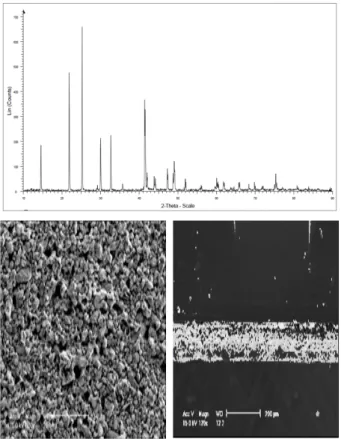
In this study, In order to evaluate the structural properties, a scanning electron microscope (SEM) and X-ray diffractometry (XRD) was used. And the
그림 4. 제작된 HgI2 필름의 XRD 패턴과 SEM 영상 Fig. 4. XRD pattern and SEM of the fabricated HgI2
film.
그림 5. 제작된 물질의 I-V 특성 Fig. 5. I-V curve of fabricated material.
leakage current was measured for the purpose of evaluating the signal-to-noise ratio. Figure 4(A) shows the XRD of fabricated HgI2 film. Figure 4(B) and (C) shows the top view and SEM image of fabricated HgI2 film. With the results, the x-ray diffraction of HgI2 film shows the preferential orientation of the peaks (101) and (102) direction and these results are in good agreement with data obtained by others. Figure 5 represent the I-V curve of fabricated material. Leakage current measurement result of the applied voltage increases, the leakage current is increased in appeared. The leakage current was 25.7 nA at an applied voltage of 50 V, respectively.
Ⅳ. Conclusion
In this paper, from a new x-ray detector that combines a columnar CsI:Na scintillation layer with a photosensitive mercuric iodide layer was investigated.
In this structure, x-rays are converted into visible light on a thick CsI:Na layer, which is then converted to electric charges in a thin HgI2 bottom layer. To optimize the thickness of phosphor coupled HgI2 multilayer structure in range of diagnostic x-ray energy, the x-ray absorption was estimated using the MCNPX. In the results of simulation, new low energy characteristic x-rays (29, 30.5, 34, 36 keV) were generated. In the case of multi-layer structure
using HgI2, the characteristic x-ray reduction is considered possible, but, reduction effect is decreased as the thickness of CsI-Na is increased. In the results of leakage current measurement, in the case of fabricated HgI2 film, leakage current increased as the applied voltage increased. The results of this research suggest that the new CsI:Na/HgI2 x-ray detector with a double-layer type structure can resolve the following problems: high voltage from the direct conversion method, and low conversion efficiency from the indirect conversion method.
REFERENCES
[1] W Que, J, A. Rowlands, X-ray imaging using
amorphous selenium: inherent spatial resolution,
Medical Physics, vol. 22, no. 4, pp. 365, 1995.[2] M. J, Yaffe, J. A. Rowlands, X-ray detectors for
digital radiography, Phys, Med. Biol. vol 42, pp.
1-39, 1997.
[3] J. K. Park, J. Y. Choi, S. S. Kang, et. al., X-ray
Sensitivity of Hybrid-type Sensor based on CaWO4-Selenium for Digital X-ray Imager,
Transactions on Electrical and Electronic Materials, vol. 5, no. 4, pp. 133, 2004.[4] Fiorini. C, Longoni. A, Perotti. F, et. al.,
Detectors for high resolution gamma-ray imaging based on a single CsI(TI) scintillator coupled to an array of silicon drift detectors, J.
of IEEE, vol. 1, no. 1, pp. 10, 2001.
[5] S. O. Kasap, and J. A. Rowlands,
Photoconductor selection for digital flat panel x-ray imaging detectors based on the dark current, J. Vac. Sci. Technol., vol. 18, no. 2, pp.
615, 2000.
[6] S. S. Kang, J. H. Kim, H. W. Lee, et. al., X-ray
response characteristic of Zn in the polycrystalline Cd1-xZnxTe detector for digital radiography,
Transactions on Electrical and Electronic Materials, vol. 3, no. 2, pp. 28, 2000.[7] S. H. Kim, C. M. Kim, K. C. Nam, et. al., Study
of The Amorphous Selenium (a-Se) using 2-dimensional Device Simulator, Journal of The
Institute of Electronics Engineers of Korea, vol.49, no. 10, pp. 187-193, 2012.
저 자 소 개 박 지 군(정회원)
2000년 인제대학교 의용공학과 석사 졸업
2003년 인제대학교 의용공학과 박사 졸업.
2008년∼현재 한국국제대학교 방사선학과 조교수
<주관심분야 : 디지털 방사선 검출기, 방사선 검 출 센서>
정 봉 재(정회원)
1998년 한국방송통신대학교 경영학과 학사 졸업.
2001년 경남대학교 경영대학원 석사 졸업.
2011년 고신대학교 보건과학과 박사 졸업.
2011년∼현재 한국국제대학교 방사선학과 조교수
<주관심분야 : 영상처리, 의료영상처리, 초음파>
최 일 홍(정회원)
1983년 명지대학교 전자공학과 학사 졸업.
1985년 명지대학교 전자공학과 석사 졸업.
1998년 명지대학교 전자공학과 박사 졸업.
1992년∼현재 한국국제대학교 방사선학과 교수
<주관심분야 : 생체신호처리, 방사선 계측>
노 시 철(정회원)-교신저자 2002년 인제대학교 의용공학과
학사 졸업.
2004년 인제대학교 의용공학과 석사 졸업.
2011년 인제대학교 의용공학과 박사 졸업.
2011년∼현재 한국국제대학교 방사선학과 조교수
<주관심분야 : 의료용 초음파, 생체신호처리, 생 체자극 시스템, 재활공학>