ISSN: 1226-7244 (Print) ISSN: 2288-243X (Online) 논문번호 16-02-06
41
j.inst.Korean.electr.electron.eng.Vol.20,No.2,163∼166,June 2016 http://dx.doi.org/10.7471/ikeee.2016.20.2.163
A Study on Temperature Dependent Super-junction Power TMOSFET
Young Hwan Lho*★
Abstract
It is important to operate the driving circuit under the optimal condition through precisely sensing the power consumption causing the temperature made mainly by the MOSFET (metal-oxide semiconductor field-effect transistor) when a BLDC (Brushless Direct Current) motor operates. In this letter, a Super-junction (SJ) power TMOSFET (trench metal-oxide semiconductor field-effect transistor) with an ultra-low specific on-resistance of 0.96 mΩ· under the same break down voltage of 100 V is designed by using of the SILVACO TCAD 2D device simulator, Atlas, while the specific on-resistance of the traditional power MOSFET has tens of mΩ·, which makes the higher power consumption. The SPICE simulation for measuring the power distribution of 25 cells for a chip is carried out, in which a unit cell is a SJ Power TMOSFET with resistor arrays. In addition, the power consumption for each unit cell of SJ Power TMOSFET, considering the number, pattern and position of bonding, is computed and the power distribution for an ANSYS model is obtained, and the SJ Power TMOSFET is designed to make the power of the chip distributed uniformly to guarantee it’s reliability.
Key words: MOSFET, BLDC motor, on-resistance, Super-junction TMOSFET, breakdown voltage
* Dept, of Railroad Electricity, Woosong University
★ Corresponding author
e-mail ; [email protected], 042) 629-6731
※ Acknowledgment
This work was supported by Institute for Information & Communications Technology Promotion (IITP) grant funded by the Korea government (MSIP) (No. B0186-16-1001. Form factor-free Multi-input and output Power Module Technology for Wearable Devices).
Manuscript received Mar, 16. 2016; revised May. 10, 2016; accepted May. 11, 2016
This is an Open-Access article distributed under the terms of the Creative Commons Attribution Non-Commercial License(http://creativecommons.org/licenses/by-nc/3.0) which permits unrestricted non-commercial use, distribution, and reproduction in any medium, provided the original work is properly cited.
I. Introduction
For a conventional MOSFET, there is a trade -off between specific on-state resistance ( ) and breakdown voltage (). In order to overcome the trade-off, a SJ (super- junction) power TMOSFET (trench metal-oxide semiconductor field-effect transistor) structure [1]
is proposed, which has P and N pillars with equal widths, and , respectively. The relationship between the doping concentrations and widths of the pillars is as follows.
(1)
where and are the doping concentrations of the P and N pillars in an SJ TMOSFET, respectively.
In the SJ TMOSFET, the breakdown voltage is proportional to the length of the drift region of
as shown in Eq. (2).
(2)
where is the critical electric field.
(163)
42 j.inst.Korean.electr.electron.eng.Vol.20,No.2,163∼166,June 2016
II. SJ TMOSFET with Temperarute Sensor
1. On-resistance
The on-resistance [1] of an SJ TMOSFET can be determined by currents flowing from the channel between the source and the drain electrodes, which is consisted of 6 types.
Channel resistance and drift region resistance mainly affect on-resistance, and the other types of resistance can be quantitatively ignored.
The channel resistance is given by
n i
(3)
where is the channel length, is the width of unit cell, n i is the channel electron mobility, is the channel gate capacitance,
is the gate voltage, and is the threshold voltage.
The drift region resistance contributed from the mesa region can be computed by considering a small segment of the drift region at a depth from the bottom of the gate electrode. The drift resistance of the drift region is obtained by
(4)
where is the cell width, is the width of N pillar, is the length of the drift region,
is the charge, is the channel electron mobility, and is the doping density of the drift region. An additional drift resistance of
in the TMOSFET structure is
considered as the buffer layer positioned below the bottom of the trenches.
(5)
2. Temperature Sensor
For temperature sensing, the temperature change
of the base-emitter voltage () under a constant emitter current is measured.
(6)
where is the temperature dependent base-emitter voltage, is the reference temperature, and
is the temperature coefficient of -2 mV/K [2].
The relationship between power and temperature is given by
× (7)
where and represent junction and case temperature, respectively, indicates power, and
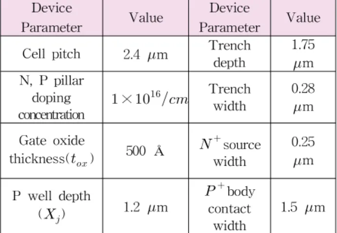
represents thermal resistance. The main characteristics of an SJ TMOSFET with bipolar sensor are shown in Table 1.
Table 1. Specifications of SJ TDMOSFET Device
Parameter Value Device
Parameter Value Cell pitch 2.4 m Trench
depth
1.75
m N, P pillar
doping concentration
× Trenchwidth 0.28m
Gate oxide
thickness() 500 Å source width
0.25
m
P well depth
() 1.2 m
body contact
width
1.5 m
The structure of SJ TMOSFET [3] with diode type temperature sensor is shown in Fig. 1, and the cross section [4] is designed in Fig. 2.
Fig. 3 shows the vertical doping profile for the cathode layer, which is consistent to the design parameter of × . The breakdown voltage of 132 V, which is composed of 33 contour lines with 4 V each line and met with the design specification, is obtained as shown in Fig. 4.
(164)
A Study on Temperature Dependent Super-junction Power TMOSFET 43
Fig. 1. Structure of SJ TMOSFET.
Fig. 2. Design of SJ TMOSFET
Fig. 3. Vertical doping profile from top to bottom of the cathode.
Fig. 4. Potential distribution when Vdrain is 132V.
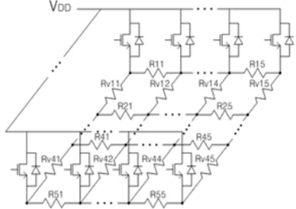
The simulation circuit is consisted of 5×5 SJ TMOSFETs and 4×4 arrays. Every node point at the resistor array located at the source metal is connected to the source. The area of the chip is 1 , and the drift resistance between grid points is calculated to be about 25 mΩ and the resistance of bonding wire is 0.1 mΩ.
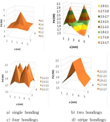
The power dissipation [5-7] becom es both w idely and uniformly distributed as the number of bonding wires increases. The power is more widely dispersed in the stripe bonding structure case, which is similar to four bondings, than one and
Fig. 5. Equivalent resistance model of 5×5 SJ TMOSFETs arrays.
two bondings. The power dissipations for the various different bonding schemes are shown in Fig. 6. For a single bonding wire, the maximum and minimum powers are measured as 4.38 W and 1.57 W, respectively. Similarly, the values for two bondings are 2.93 W and 1.57 W. In the case of four bonding wires, the maximum power of 2.38 W and the minimum of 2.69 W are obtained, respectively. These values are similar to those of the stripe bonding in Fig. 6. A SPICE [8] self-heating electro-thermal model from the Fairchild TO220 package is applied.
(165)
44 j.inst.Korean.electr.electron.eng.Vol.20,No.2,163∼166,June 2016
a) single bonding b) two bondings c) four bondings d) stripe bondings
Fig. 6. Power distributions of 5×5 array meshes for different bondings.
III. Conclusion
The SJ TMOSFET with an embedded temperature sensor was successfully designed to meet the breakdown voltage of 100 V class and an ultra-low specific on-resistance of 0.96 Ω· for a BLDC motor.
When assembling the SJ TMOSFET, the number of bonding wires and their positions should be considered dispersing the hot spot area locating near the bonding area. The hot spot area is dispersed as the number of bonding wires increases, and the stripe bonding type shows a suitable effective SJ TMOSFET package.
References
[1] B. J. Baliga, “Advanced Power MOSFET Concepts,”
NY. USA: Springer-Science, pp.265-354, 2010.
[2] H. Kock et. al., “Design of a test chip with small embedded temperature sensor structures realized in a common-drain power trench
technology,” IEEE Conference on Microelectronic Test Structure, Amsterdam, The Netherlands, April 4-7, pp. 176-181, 2011.
[3] Young Hwan Lho, “Design of Super-junction TMOSFET with Embedded Temperature Sensor”, Vol. 19, No. 2, Journal of Korean Electrical and Electronics Engineers, pp. 232-236, June 2015.
[4] SILVACO TCAD Manual, Atlas, 2011
[5] H. Dia, “A temperature dependent power MOSFE T model for switching application,” Thermal Investigation of ICs and Systems, THERMI NIC International Workshop on, pp.
87- 90, 7-9, Oct. 2009.
[6] Stefano de Filippis, et. al., “ANSYS based 3D electro-thermal simulations for the evaluation o f power MOSFETs robustness,” Microelectroni cs Reliability 51, pp. 1954-1958, 2011.
[7] Messaadi Lofti, et. al., “The Electro-Thermal Subcircuit Model for Power Mosfets,” Microelectronic s and Solid State Electronics, 1(2), pp. 26-32,
2012.
[8] LTspice IV, Linear Technology Corporation, 2014.
(166)