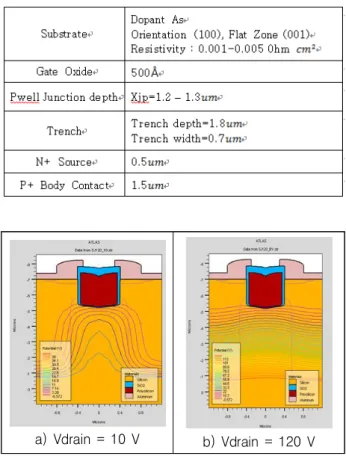
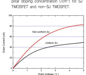
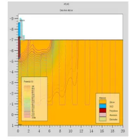
Design of Main Body and Edge Termination of 100 V Class Super-junction Trench MOSFET
5
0
0
전체 글
(2)
(3)
(4)
(5)
수치
관련 문서
