ISSN:1226-7244 (Print)
ISSN:2288-243X (Online) j.inst.Korean.electr.electron.eng.Vol.22,No.2,484∼487,June 2018
논문번호 18-02-36 http://dx.doi.org/10.7471/ikeee.2018.22.2.484
258
(484)
* Dept. of Electronic and Electrical Engineering, Hongik University
★Corresponding author
E-mail: [email protected], Tel: +82-2-320-3013.
※ Acknowledgment
This work was supported by the National Research Foundation (NRF) of Korea grant funded by the Korea government (MSIP) (NRF-2016R1A2B4010474)
Manuscript received Jun. 11, 2018; revised Jun. 26, 2018; accepted Jun. 29, 2018
This is an Open-Access article distributed under the terms of the Creative Commons Attribution Non-Commercial License
(http://creativecommons.org/licenses/by-nc/3.0) which permits unrestricted non-commercial use, distribution, and reproduction in any medium, provided the original work is properly cited.
I. INTRODUCTION
Field effect transistors (FETs) based on AlGaN/GaN heterostructure have been strong candidates for high-speed and high-power applications owing to excellent material properties such as high saturation velocity and
large breakdown voltage [1]. In addition, GaN- based devices have exhibited the potential to endure extreme environments such as an elevated temperature and high radiation [2],[3]. Radiation-abundant environment of the space requires radiation-hardened devices
5-MeV Proton-irradiation characteristics of AlGaN/GaN – on-Si HEMTs with various Schottky metal gates
Heehyeong Cho
*, Hyungtak Kim
*★Abstract
5 MeV proton-irradiation with total dose of 1015 /cm2 was performed on AlGaN/GaN-on-Si high electron mobility transistors (HEMTs) with various gate metals including Ni, TaN, W, and TiN to investigate the degradation characteristics. The positive shift of pinch-off voltage and the reduction of on-current were observed from irradiated HEMTs regardless of a type of gate materials. Hall and transmission line measurements revealed the reduction of carrier mobility and sheet charge concentration due to displacement damage by proton irradiation. The shift of pinch-off voltage was dependent on Schottky barrier heights of gate metals. Gate leakage and capacitance-voltage characteristics did not show any significant degradation demonstrating the superior radiation hardness of Schottky gate contacts on GaN.
Key words: AlGaN/GaN-on-Si, high electron mobility transistors, proton irradiation, displacement damage, Schottky contact.
---
5-MeV Proton-irradiation characteristics of AlGaN/GaN – 259 on-Si HEMTs with various Schottky metal gates
(485) in space electronics. Majority of satellites and space stations are in low earth orbital to date and protons are major species of radiation effects in this region. Previous works on the radiation response to proton irradiation reported that displacement damage is a main cause of radiation-induced degradation in GaN HEMTs [4],[5].
In this work, we fabricated AlGaN/GaN Schottky HEMTs on Si with various gate metals including Ni, TaN, W and TiN. The fabricated devices were subjected to proton irradiation with a total dose of 1015 cm-2 at 2 MeV. Moderate dependence on Schottky barrier heights (SBHs) of device degradation was observed after irradiation.
II. EXPERIMENTS
AlGaN/GaN Schottky HEMTs were fabricated on commercially available GaN-on- Si substrate. The schematic cross-sectional view of AlGaN/GaN Schottky HEMTs on Si is presented in Fig. 1. The epitaxial structure consisted of a 4.3 μm GaN buffer layer on Si (111) substrate, a 20 nm AlGaN barrier layer and a 4 nm GaN capping layer. Source/drain ohmic contacts were formed with Ti/Al/Ni/Au (20/120/25/50 nm) layers alloyed by rapid thermal annealing at 830 ℃ for 30 sec in nitrogen ambient. After active area was defined by mesa etching process, a 30 nm SiO2 was deposited by using plasma enhanced chemical vapor deposition (PECVD). Finally, Schottky metal gates were formed with Ni,
TaN, W, and TiN. Ni was deposited by e-beam evaporator and the other metals were by sputtering. The gate length (LG), gate-to-drain distance (LGD), and gate-to-source distance (LGS) were 2 μm, 15 μm, 3 μm, respectively.
Proton irradiations were performed at the Korea Institute of Radiological and Medical Sciences using an MC-50 cyclotron. The devices were irradiated at a room temperature under low vacuum atmosphere with proton energy of 5 MeV. Total proton dose was 1015 cm-2. No electrical connection was made to the devices during irradiation test.
Fig. 1 The cross-sectional view of the fabricated AlGaN/GaN HEMT on Si.
III. RESULTS AND DISCUSSION
DC I-V characteristics were measured before and after the irradiation test to investigate the proton irradiation effect. The output of AlGaN/GaN Schottky HEMTs are shown in Fig. 2 and 3, respectively. After proton irradiation, all types of devices exhibited the increase of on-resistance (RON) and the reduction of drain current in the output characteristics. The changes in specific RON of each device were summarized in Table. 1.
260 j.inst.Korean.electr.electron.eng.Vol.22,No.2,484∼487,June 2018
(486) Fig. 2 The output characteristics measured from VG = 1 to -5 V (-1 V step) before and after proton irradiation.
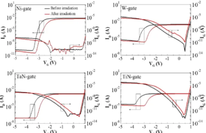
Fig. 3. The transfer characteristics measured at VD = 1 V before and after proton irradiation.
As shown in Fig. 3, the reduction of on- current and off-state leakage were also observed in the transfer characteristics of all types of devices.
Hall measurements were carried out to investigate the radiation effects on the transport properties of the electron channel at heterojunction. We measured Hall measurement patterns fabricated on the same wafer to extract Hall-mobility, sheet carrier concentration, and sheet resistance. The results are summarized in table. 2.
Table 1 The change of RON by proton irradiation.
RON
(mΩ*cm2) Ni TaN W TiN
Before
irradiation 2.59 7.41 5.43 7.1 After
irradiation 3.65 9.30 6.51 8.06
Table 2 The change of the transport parameters by proton irradiation from Hall measurements.
μ
(cm2/Vs) nsh (cm-2) Rsh (Ω/□) Before
irradiation 1700 7.7x10¹² 472 After
irradiation 1170 6.5x10¹² 816
Each parameter was degraded by proton irradiation regardless of a type of Schottky metal. Hall measurement clearly indicated that the degradation of RON and on-current should be to the degradation of the channel properties.
The degradation of electrical properties was related to proton bombardment effects in GaN- based heterostructures [6],[7].
The Schottky barrier height (SBH) was extracted from the forward I-V characteristics of Schottky gate diodes. The SBH of each type of the device was reduced after proton irradiation. The SBH reduction was inversely proportional to the magnitude of SBH. In fig. 3, a positive shift of the pinch-off voltage (Vth) was
5-MeV Proton-irradiation characteristics of AlGaN/GaN – 261 on-Si HEMTs with various Schottky metal gates
(487) observed after proton irradiation. The magnitude of the Vth shift became larger as the SBH decreases. The changes of device parameters were summarized in table 3. It suggests that radiation-hardness can be improved by employing the gate metal with a large SBH.
Table 3 The change of the SBH and Vth by proton irradiation.
metal SBH (eV) △SBH
(eV) △Vth (V)
Ni 1.09 -0.04 0.41
TaN 0.91 -0.045 0.57
W 0.85 -0.05 0.67
TiN 0.79 -0.07 0.79
IV. CONCLUSIONS
We investigated the effect of proton irradiation on AlGaN/GaN-on-Si HEMTs with Ni, TaN, W, and TiN Schottky contacts. The positive shift of Vth and the reduction of on- current were observed due to displacement damage. Hall measurements revealed that the transport properties of the electron channel were degraded by proton irradiation. The devices with the gate metal having the larger SBH demonstrated the stronger radiation resistance.
REFERENCES
[1] U. K. Mishra, et al., “AlGaN/GaN HEMTs- an overview of device operation and applications,” Proc. IEEE, vol. 90, no. 6, pp.
1022-1031, 2002. DOI: 10.1109/JPROC.2002.
1021567
[2] Y. S. Puzyrev, et al., “Radiation-Induced Defect Evolution and Electrical Degradation of AlGaN/GaN High-Electron-Mobility Transistors,”
IEEE Tran. Nucl. Sci., vol. 58, no. 6, pp. 2918- 2924, 2011. DOI: 10.1109/TNS.2011.2170433 [3] W. S. Tan, et al., “High temperature performance of AlGaN/GaN HEMTs on Si substrates,” Solid-State Electron., vol. 50, no.
3, pp. 511-513, 2006. DOI: 10.1016/j.sse.2006.
02.008
[4] G. Sonia, et al., “2 MeV ion irradiation effects on AlGaN/GaN HFET devices,” Solid- State Electron., vol. 52, no. 7, pp. 1011-1017, 2008. DOI: 10.1016/j.sse.2008.02.005
[5] X. Hu, et al., “Proton-Irradiation Effects on AlGaN/AlN/GaN High Electron Mobility Transistors,” IEEE Tran. Nucl. Sci., vol. 50, no.
6, pp. 1791-1796, 2003. DOI: 10.1109/TNS.
2003.820792
[6] Dong-Min Keum, et al., “Proton Bombardment Effects on Normally-off AlGaN/GaN-on-Si Recessed MIS Heterostructure FETs,” IEEE Trans. Nucl. Sci., vol. 62, no. 6, pp. 3362-3368, 2015. DOI: 10.1109/TNS.2015.2495209
[7] C.F. Lo, et al., “Effects of proton irradiation on dc characteristics of InAlN/GaN high electron mobility transistors,” J. Vac. Sci.
Technol. B, vol. 29, pp. 061201-1-061201-6, Sep., 2011. DOI: 10.1116/1.3644480