1. Introduction
In the design of semiconductor integrated circuits, ESD is one of the important issues related to product quality improvement and reliability. Especially, ESD is recognized as an important problem of integrated circuit design due to process development and reduction of thickness of gate oxide. Many ESD protection circuits have been studied to solve such ESD problems[1]. Recently, research on SCR has been actively conducted with ESD protection devices because it has electrical characteristics that can drive large currents even in a smaller area than the ggNMOSFET used as an ESD protection
device[2~5]. However, due to the nature of the structure, the SCR can have undesirable latch-up problems due to overshoot voltage and noise other than ESD in normal operating conditions due to its low triggering voltage(<2V) and high trigger voltage above 20V[5]. To avoid this, some SCR-based devices also benefit from external circuitry to achieve low trigger voltage and high holding voltage[6].
The proposed device can protect the gate oxide of the internal circuit with the low trigger voltage by modifying the existing SCR structure without adding the external circuit, and it is possible to prevent undesired latch-up phenomenon in the steady state due to the
New Thyristor Based ESD Protection Devices with High Holding Voltages for On-Chip ESD Protection Circuits
Suen-Ki Hwang*, Ha-Young Cheong**
Abstract In the design of semiconductor integrated circuits, ESD is one of the important issues related to product quality improvement and reliability. In particular, as the process progresses and the thickness of the gate oxide film decreases, ESD is recognized as an important problem of integrated circuit design. Many ESD protection circuits have been studied to solve such ESD problems. In addition, the proposed device can modify the existing SCR structure without adding external circuit to effectively protect the gate oxide of the internal circuit by low trigger voltage, and prevent the undesired latch-up phenomenon in the steady state with high holding voltage.
In this paper, SCR-based novel ESD(Electro-Static Discharge) device with the high holding voltage has been proposed. The proposed device has the lower triggering voltage without an external trigger circuitry and the high holding voltage to prevent latch-up phenomenon during the normal condition. Using TCAD simulation results, not only the design factors that influence the holding voltage, but also comparison of conventional ESD protection device(ggNMOS, SCR), are explained. The proposed device was fabricated using 0.35um BCD process and was measured electrical characteristic and robustness. In the result, the proposed device has triggering voltage of 13.1V and holding voltage of 11.4V and HBM 5kV, MM 250V ESD robustness
Key Words : ESD Protection Device, TCAD, ggNMOS, BCD, SCR, HBM 5kV
*Dept. of Smart Electronics, Yeongju Campus of KOREA POLYTECHNICS
**Kyonggi university graduate school
Received April 12, 2019 Revised April 18, 2019 Accepted April 18, 2019
high holding voltage.
2. Main subject
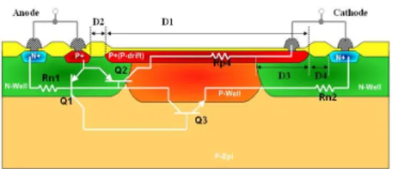
2.1. New ESD Protection Device Structure The proposed device modifies the structure of MVTSCR (Middle Voltage Trigger SCR) modified from the existing SCR, inserts p-drift junction between n-well and p-well, and inserts n- Respectively It is shown in Fig1.
Fig. 1. Cross section of the proposed device and equivalent circuit
The operation principle of this device can be explained by the operation of NPN / PNP which occurs in the same parasitic as the existing SCR. That is, when the anode voltage becomes larger than the trigger voltage of the SCR, the PNP-BJT is turned on, and a part of the current flowing into the anode drifts through the n-well to flow through the p-well to the p + cathode. At this time, if the current passing through the p-well increases due to the resistance of the p-well, the emitter-base junction (EBJ) of the NPN-BJT changes to the forward bias state and turns on. The collector current of the NPN flowing from the n-well to the cathode becomes the base current of the PNP to sustain the operation of the PNP.
Similarly, the collector current of the PNP becomes the base current of the NPN so that both BJTs perform the forward feedback operation. ] [3] The trigger voltage of the conventional SCR is determined by the
avalanche breakdown between the n-well and the p-well In order to lower the trigger voltage, a p + (p-drift) junction was added between the n-well and the p-well to lower the trigger voltage by lowering the blocking junction between the n-well and the p-well. The holding voltage can be described as the voltage drop between the anode and the cathode when two BJTs (NPN / PNP) are triggered and operated.
The holding voltage is dependent on the degree of space charge neutrality in the two BJT base regions and on the emitter injection efficiency.
Therefore, to increase the holding voltage, the proposed device increased the holding voltage by optimizing D1, D2 shown in Fig. 1 related to the base region and D3, D4 related to the emitter injection efficien.
2.2. Simulation of the proposed device The TCAD simulator was used to analyze the trend of the electrical characteristics of the proposed device through device simulation, and the comparison with the existing ESD protection device was analyzed by the mixed mode simulation. Figure 2 shows the electrical characteristics of the device and the voltage clamping and temperature at HBM 4K
(A)
(B)
Fig. 2. (A) DC I-V characteristics with existing devices, (B) Voltage and temperature characteristics at HBM 4K
The trigger voltage of the proposed device in Fig. 2. (A) is 11.5V similar to ggNMOS. The holding voltage is 4V higher than the holding voltage (1.8V) of the conventional SCR. Figure 2 (B) shows the voltage clamping and lattice temperature when the HBM 4 kV stress is applied and the device size is 100 μm. The proposed device has a temperature similar to that of the existing SCR, which is lower than the ggNMOS when the voltage is clamped. This results in high holding voltage and high ESD performance.
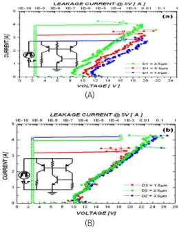
Fig. 3. DC-IV characteristics of proposed device according to design variables (D1, D2, D3, D4)
3. Fabrication and measurement results of the proposed device
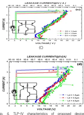
The proposed device was fabricated with 0.35um BCD process for the compatibility of
low voltage and high voltage with the size of 50um. The I-V characteristics were measured with a TLP tester and ESD tolerance characteristics (HBM, MM) were measured with ESS-6008. Figure 4 shows the TLP-IV characteristics of the proposed device according to design variables. As shown in Fig.
4, the measured results of the proposed device show the same characteristics as the trend of simulation. The higher the holding voltage, the lower the secondary breakdown current, ie ESD tolerance. This can be explained by equation (1). The higher the holding voltage, the lower the secondary breakdown voltage.
× (1)
Therefore, the power consumed by the ESD protection device is lowered and the ESD tolerance characteristic is lowered.
(A)
(B)
(C)
Fig. 4. TLP-IV characteristics of proposed device according to design variables (D1, D2, D3, D4)
In addition, the ESD tolerance characteristics of the proposed device were measured with HBM 5KV, MM 200V. Table 1 summarizes the ESD performance characteristics of the proposed device
Table 1. Characteristics of proposed ESD protection device
division variable Measures
Electrical characteristic VT1 13.1V Electrical characteristic IT1 3.68mA Electrical characteristic VH 11.4V Electrical characteristic IH 3.02A Electrical characteristic HBM 5KV Tolerance characteristic MM 250V
Ⅴ. conclusion
In this study, we propose a novel thyristor - based ESD protection device with high holding voltage and verify the electrical characteristics of the proposed device through simulation and then measure and analyze electrical
characteristics and endurance characteristics.
The proposed device has a trigger voltage of 13.1V and a latching voltage of 10V or more. In addition, ESD tolerance characteristics of HBM 5KV and MM 250 have large ESD performance with small area.
REFERENCES
[1] R. G Wagner, J. Soden and C.F. Hawkins &
quot; Extend and Cost of EOS / ESD Damage in an IC Manufacturing Process &
quot ;, in Proc. of the 15th EOS / ESD Symp., pp. 49-55, 1993.
[2] A. Amerasekera and C. Duvvury ESD in silicon integrated circuits, Wiley, New York 2005
[3] Chris Toumazou, “Trade-Offs in analog Circuit Design” Kluwer Academic Publishers, 139p-2004p
[4] Baker, "CMOS Circuit Design and layout", Wiley, 900p
[5] K. Mark Smith, Jr., “A Comparison of Voltage-Mode Soft-Switching Methods for PWM Converters” IEEETrans-Power Electronic, Vol. 12, No. 2 (1997)
[6] A. Djemouai,, "New CMOS Integrated Pulse Width Modulator for Voltage Conversion Applications", IEEE 0-7803-6542-9(2000) [7] Lu Chen,, "Design and Test of a
Synchronous PWM Switching Regulator System", IEEE 0-7803-6253-5(2000)
저자약력
황 선 기(Suen-Ki Hwang) [종신회원]
• 1997년 서울산업대학교 전자 공학과 학사
• 2000년 동의대학 산업대학원 석사
• 2007년 관동대학교 일반대학 원 박사과정
<관심분야> 영상처리 및 신호처리시스템
정 하 영(Ha-Young Cheong) [종신회원]
• 1984년 2월 : 경기대학교 산업공 학과 (공학사)
• 2010년 8월 : 가톨릭관동대학교 전자통신공학과 (공학박사)
<관심분야> 실시간 인식 및 추적 시스템