Design of the power generator system for photovoltaic modules
Sung-Joon Park*★
Abstract
In this paper, a dc-dc power converter scheme with the FPGA based technology is proposed to apply for solar power system which has many features such as the good waveform, high efficiency, low switching losses, and low acoustic noises. The circuit configuration is designed by the conventional control type converter circuit using the isolated dc power supply. This new scheme can be more widely used for industrial power conversion system and many other purposes. Also, I proposed an efficient photovoltaic power interface circuit incorporated with a FPGA based DC-DC converter and a sine-pwm control method full-bridge inverter. The FPGA based DC-DC converter operates at high switching frequency to make the output current a sine wave, whereas the full-bridge inverter operates at low switching frequency which is determined by the ac frequency. As a result, we can get a 1.72% low THD in present state using linear control method. Moreover, we can use stepping control method, we can obtain the switching losses by Sp measured as 0.53W.
This paper presents the design of a single-phase photovoltaic inverter model and the simulation of its performance.
Key words: DSC, photovoltaic, photovoltaic power generator
* Power Generation Division, Korea Hydro-Nuclear Power
★Corresponding author
I. Introduction
Recently, there are many researches about the alternate energy sources as the increase of the concern about the global environment protection and the demand for the pollution-free natural energy.
We have already been confronted with serious global environmental problem, such as Greenhouse effect and environmental pollution. To overcome these problems, development of renewable, clean energy technologies which include photovoltaic, solar thermal, wind turbines, hydro-power, wave and tidal power etc. are imperative common challenges for mankind to live in the future[1]-[2].
Especially, the solar energy is one of the positive
choices. Above all, dye sensitized solar cells(DSC) are expected to become popular solar cells because of their advantages of cost and efficiency. A photovoltaic system consists of solar cells and ancillary components such as power-conditioning equipment and support structures. Solar cells utilize the energy from the sun by converting solar radiation directly into electricity. The potential of the sun as an energy resource is enormous as about 1×10¹⁸ kWh strike the earth's surface yearly.
This can be compared to the total world energy consumption of 1×10¹⁴ kWh in 2000.
In this study, the 50W load connected solar power system is schematically classified into three different types; an alternative three-phase full bridge switching, an isolated high frequency transformer DC link and a transformer-less direct AC link. The topologies of three-step shifter dc-dc converter are
advantageous for safety and reliable viewpoint due to the function of exact gate signal. Also, there is a fascination about it because of lower hysteresis loss, mutual inductance and high frequency scheme. This method is used for the transformer magnetic circuit to reduce the core losses. This paper presents a high frequency transformer connected three-step phase-shifted technology by using FPGA interface to personal computer for the residential PV power system, which delivers the single-phase 2 wire type 60Hz AC output into the AC power grid[3]. And we also describe the whole system configuration of a new utility interactive DC modulated converter for solar power system with a high solar energy conversion efficiency. Its operating principle and related RTOS(real time operating system) computer control schemes areproposed from an experimental point of view.
II. Real photovoltaic modeling of the PV modules
Fig. 1 represents the simplified equivalent electric circuit of a PV module defined by the following equations[4]:
I= I SC[1- exp ( V+ VOC+IRS
Vt )-1]- V+RSI RP (Eq-1)
Vt= mkTq (Eq-2)
where I, V are the PV module output voltage and current, ISC is the ideal PV module short-circuit (A), VOC is the ideal PV module open-circuit voltage (V), Vt is the thermal voltage (V), m is a nonideality factor, k is the Boltzmann constant, T is the absolute cell temperature (K), q is the electron charge and RS, RP are the series and parallel resistance, respectively, of the PV module.
RP Solar Energy
RS
Vs
+
-
I
V +
- RP
Solar Energy
RS
Vs
+
-
I
V +
-
Fig. 1. The PV module equivalent circuit.
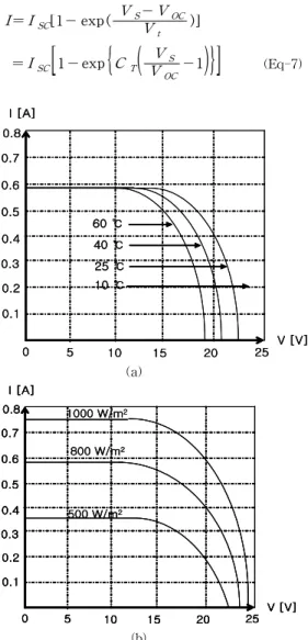
The I-V characteristics of a commercially available PV module for various cell temperature and incident solar irradiance conditions are shown in Fig. 2(a and b), respectively. The short-circuit current, ISC, is proportional to the solar irradiance, G(W/㎡), incident on the module, while the open-circuit voltage, VOC, is usually considered to depend only on the PV module cell temperature, TC (℃), thus neglecting the effect of the incident solar irradiance on the open-circuit voltage[5]:
ISC=ISC.STC G
1000W/㎡ (Eq-3)
VOC=VOC.SOC-KT(TC-25℃) (Eq-4) TC=T-273K= TA+ NOCT - 20℃800W/㎡ G (Eq-5) where, ISC.STC is the short-circut current (A) under standard test conditions (STC, cell temperature = 2 5℃ and solar irradiance = 1kW/㎡), VOC.STC is the open-circuit voltage (V) under STC, KT is the open-circuit voltage temperature codfficient (V/℃), TC is the cell temperature (℃), TA is the ambient temperature (℃) and NOCT is the normal operating cell temperature(℃). The values of ISC.STC, VOC.STC, KT and NOCT are specified by the PV module manufacturer. The effect of the cell temperature on the short-circuit current is assumed negligible.
The effect of the parallel resistance, RP, is usually neglected, resulting in the following, simplified, I-V characteristic equation:
I = ISC[1- exp ( V- VOC+IRS
Vt )] (Eq-6)
The PV module mathematical modeling presented above, has the drawback that the output current , I,
appears on both sides of Equations. (Eq-1) and (Eq-6). In order to avoid the corresponding calculation complexity, in this charter, the ideal PV module output current is calculated as follows[6]:
I = ISC[1- exp ( VS-VOC
Vt )]
=ISC
[
1 - exp{
CT(
VVOCS -1)}]
(Eq-7)0.7 0.6 0.5 0.4 0.3 0.2 0.1 0.8
0 5 10 15 25
60 ℃ 40 ℃
20 25 ℃
10 ℃
V [V]
I [A]
0.7 0.6 0.5 0.4 0.3 0.2 0.1 0.8
0 5 10 15 25
60 ℃ 40 ℃
20 25 ℃
10 ℃
V [V]
I [A]
(a)
0.7
0.6
0.5
0.4
0.3
0.2
0.1 0.8
0 5 10 15 20 25
V [V]
I [A]
500 W/m2 800 W/m2 1000 W/m2 0.7
0.6
0.5
0.4
0.3
0.2
0.1 0.8
0 5 10 15 20 25
V [V]
I [A]
0.7
0.6
0.5
0.4
0.3
0.2
0.1 0.8
0 5 10 15 20 25
V [V]
I [A]
500 W/m2 800 W/m2 1000 W/m2
(b)
Fig. 2. The current-voltage characteristics of a PV module with temperature and irradiance.
C(T)= VVOC
t (Eq-8) 0≤VS≤VOC (Eq-9) where VS is the ideal PV module output voltage.
Using the values of I calculated using, Eq.(Eq-7), the corresponding values of the PV module output
voltage, V , are calculated using the following equations:
V=VS-IRS (Eq-10) 0≤ V≤ VOC (Eq-11)
Considering the values of VOC and Vt for various commercially available PV modules, operating under the temperature conditions of typical PV energy production applications, the temperature sensitivity of CT in Eq. (Eq-7) is neglected in the proposed method. The ideal PV module modeling based on this approximation has the advantage of reduced calculation complexity[7].
Ⅲ. Converter design concept As illustrated in Fig. 3, the proposed PV simulator is composed of two subsystem:
(ⅰ) the switched-mode DC/DC power converter and (ⅱ) the control system, consisting of the FPGA unit, the analog to digital(A/D) converters and the voltage and current sensors.
Fig. 3. The block diagram of the PV module.
The power converter input voltage, Vin, is an unregulated DC voltage. A constant frequency duty control signal, Vm , depicted in Fig. 4(a), is producted by the FPGA unit and it is used to control the power switch, S, in order to modulate the DC input voltage into a high-frequency wave, Voi, shown in Fig. 4(b), which then passes through a lowpass L-C filter producing the DC output voltage, VO. The DC output voltage is regulated to the desired value by adjusting the duty signal duty cycle value, D, as follows:
ton toff Ts
t
0
Vm
ton toff Ts
t
0
Vm
(a)
ton toff
Ts
t
0
Voi
Vin Vo
ton toff
Ts
t
0
Voi
Vin Vo
(b)
Fig. 4. The DC to DC converter principal waveform
VO=DVIN= tON
TS VIN (Eq-12) where ton is the duty signal ON time and TS is the switching period.
The switching frequency is adjusted by the VOand DC converter out voltage. The comparator sends a signal to ROM in FPGA. The interval for dc-dc step converter is determined by the signal of the reference value comparing with the DC voltage.
The appropriate frequency from that is also sent to the FPGA. The main elements of the driving signal are designed to diminish the saturation energy. The control circuit consists of three part. One is computer keyboard for being taken information of desirable duty ratio and frequency.
To drive dc-dc converter, we can determine duty ratio and frequency. Another is duty ratio and switching frequency display part to show operational time in PC monitor.
The resulting output voltage and current measurements are interfaced in digital format to the FPGA unit through the corresponding 8-bit A/D converters.
The DC/DC converter output voltage and current are related, in case of ohmic load, according to the linear
The simulated PV module I-V characteristic, which is calculated by the control circuit implemented in the FPGA unit.
Fig. 5 shows the controller circuit schematic for dc-dc converter. This controller is digitally implemented on the FPGA(ACEX-EP1K100_208PQFP type) and interfaced with PC parallel port. The on-board clock running at 12MHz was used. An over-current detection faculty is added to protect the system under fault situations.
Fig. 5. Controller circuit for dc-dc converter.
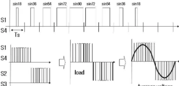
Ⅲ. inverter design concept Fig.6 shows waveforms of the proposed sine-pwm.
Because duty is controlled by sine wave, it is reduced harmonics distortion and increased power efficiency.
Fig. 6. Gate signal waveforms of sine PWM method.
(a)
(b)
Fig. 7. The output waveform: (a) linear PWM inverter, (b) sine-PWM inverter.
Fig. 7(a) shows the waveform used for the linear control PWM. Fig. 7(b) presents the waveform of sine PWM method.
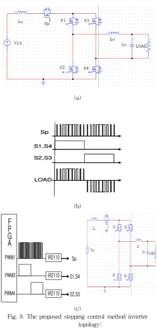
Also, I propose a photovoltaic module inverter system using stepping control method and full-bridge circuit. Fig 8(a) shows the structure of a proposed interface circuit. It consists of five switches, an inductor, and LC filter at output port. Sp operates at a high switching-frequency to make the output current a sinusoidal wave, and S1~S4 switches determine the polarity of the ac output voltage.
Therefore, compared with general full-bride PWM inverter that performance complete chopping, this system reduces the switching loss.
Fig. 8(b) shows the operational waveform for each input gate signal(Sp, S1~S4).
As shown in Fig. 8(b), during a positive half cycle of the ac utility voltage, the polarity selection, S1 and S4, are conducting, and a pulse width modulated switching signal to synthesize a sinusoidal current wave is applied to Sp. In contrast, a case where S2 and S3 are conducting, the current obtained by the dc-dc converter is transferred to the negative direction of the utility line voltage.
The control signal is shown in Fig. 8(c). It shows
gate signals of Sp and S1~S4 from FPGA. By using this programming digital circuit, it can determine the switching sequence of the full-bridge switches.
(a)
Sp
S1,S4
S2,S3
LOAD Sp
S1,S4
S2,S3
LOAD
(b)
Sp S1,S4 S2,S3 PWM1
PWM3 PWM4
FP GA
IR2110 IR2110
IR2110 (c)
Fig. 8. The proposed stepping control method inverter topology:
(a) Stepping control method inverter, (b) Gate singal waveforms Sp, S1~S4.
(c) Stepping drive inverter circuit and control signal.
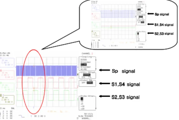
Fig. 9 shows FPGA output signal. In this signal waveform, the switching patterns of the controlled switches S1~S4 are decided by its direction. When S1
and S4 is turn on, S2 and S3 is fully trun off. In order to voltage change, the switching pattern is reversed, switches S1 and S4 is turn off, S2 and S3 is turn on.
Sp signal Sp S1,S4 signal S1,S4 S2,S3 signal S2,S3
Sp signal Sp
S1,S4 signal S1,S4 S2,S3 signal S2,S3
Sp signal Sp S1,S4 signal S1,S4 S2,S3 signal S2,S3
Sp signal Sp
S1,S4 signal S1,S4 S2,S3 signal S2,S3
Fig. 9. Experimental gate signal.
Fig. 10 shows simulation waveform and experimental waveform. These experimental results are similar to simulations results. As we can use sine PWM control method, we can get a 1.72% low THD in present state using linear control method. Moreover, we can use stepping control method, we can obtain the switching losses by Sp measured as 0.53W.
a. 실제 LOAD에 걸리는 전압이 낮다.
b. 파형의 형태가 고르지 못하다.
Fig. 10. The proposed inverter output waveform: (a) simulation waveform,
(b) experimental waveform
4. Results and discussion
In this study, I proposed an efficient photovoltaic power interface circuit incorporated with a FPGA based DC-DC converter and a sine-pwm control method full-bridge inverter.
We have investigated operational characteristics of this solar power system as a function of FPGA based controller.
As a result, we can get a 1.72% low THD in present state using linear control method. Moreover, we can use stepping control method, we can obtain the switching losses by Sp measured as 0.53W.
References
[1] Internatinal Energy Agency, "Trends in Photovoltaic applications, In selected IEA countries between 1992 and 2001, in Photovoltaic Power systems Programme", Report IEA PVPST1-11, 2002.
[2] International Energy Agency, "Key World Energy Staticstics", 2002.
[3] Hee-Chang Lee and Sung_Joon Park, "A new proposal of three-step dc-dc converter scheme for solar power system", International Journal of KIMICS, vol. 5, No.4, December 2007 [4] A.K. Mukerjee, N. Dasgupta, "DC power supply
used as photovoltaic simulator for testing MPPT algorithms", Renewable Energy vol. 32, pp 587-592, 2007
[5] Eftichios Koutroulis, Kostas Kalaitzakis, Vasileios Tzitzilonis, "Development of an FPGA-based
system for real-time simulation of photovoltaic modules", in-press of Microelectronics Journal, 11 July 2008
[6] P. Sanchis, J. Lopez, A. Ursua, L. Marroyo,
"Electronic controlled device for the analysis and design of photovoltaic systems", IEEE Power Electron. Lett. 3, pp 57-62, 2005
[7] K. Khouzam, K. Hoffman, "Real-time simulation of photovolaic modules", Sol. Energy 56, pp 521-526, 1996
BIOGRAPHY
Sung-Joon Park
2000 : BS degree in Electrical Engineering, Dongui University.
2002 : MS degree in Electrical Engineering Engineering, Pusan National University.
2008 : He is currently working toword a Ph.D. in Electrical Engineering, Pusan National University.
2002~2003 : Research Engineer, LG Electronics Institute of Technology.
2004~2008 : Korea Hydro-Nuclear Power Company.
![Fig. 1 represents the simplified equivalent electric circuit of a PV module defined by the following equations[4]: I= I SC [1- exp ( V+ V OC + IR S V t )-1]- V+R S IRP (Eq-1) V t = mkT q (Eq-2)](https://thumb-ap.123doks.com/thumbv2/123dokinfo/4680917.502006/2.772.400.700.161.297/represents-simplified-equivalent-electric-circuit-defined-following-equations.webp)