[논 문] 한국재료학회지 http://dx.doi.org/10.3740/MRSK.2011.21.9.482 Kor. J. Mater. Res.
Vol. 21, No. 9 (2011)
482
†Corresponding author
E-Mail : [email protected]. (H. -J. Sun)
Thermal Instability of La
0.6Sr
0.4MnO
3Thin Films on Fused Silica
Ho-Jung Sun
†Department of Materials Science and Engineering, Kunsan National University, Kunsan 573-701, Korea
(Received June 1, 2011 : Received in revised form August 3, 2011 : Accepted August 5, 2011)
Abstract
La0.6Sr0.4MnO3 (LSMO) thin films, which are known as colossal magnetoresistance materials, were prepared on fused silica thin films by conventional RF magnetron sputtering, and the interfacial reactions between them were investigated by rapid thermal processing. Various analyses, namely, X-ray diffraction, transmission electron microscopy combined with energy adispersive X-ray spectrometry, and secondary ion mass spectrometry, were performed to explain the mechanism of the interfacial reactions. In the case of an LSMO film annealed at 800oC, the layer distinction against the underplayed SiO2 was well preserved. However, when the annealing temperature was raised to 900oC, interdiffusion and interreaction occurred. Most of the SiO2 and part of the LSMO became amorphous silicate that incorporated La, Sr, and Mn and contained a lot of bubbles.When the annealing temperature was raised to 950oC, the whole stack became an amorphous silicate layer with expanded bubbles. The thermal instability of LSMO on fused silica should be an important consideration when LSMO is integrated into Si-based solid-state devices.
Key words
La0.6Sr0.4MnO3, fused silica, thin film, interfacial reaction.1. Introduction
La
1-xSr
xMnO
3is a manganite known as a colossal mag- netoresistance material. It has useful magnetic and elec- trical properties,
1,2)thus it can be used as a key component for spintronic devices.
2,3)Its good electrical conductivity and structural compatibility with perovskite-structured functional materials give it the potential to be used as electrodes in integrated solid-state devices.
4,5,6)For its use in integrated circuits (ICs), La
1-xSr
xMnO
3should be prepared as a thin film. Many studies have been executed to fabricate La
1-xSr
xMnO
3thin films by using various preparation routes.
7,8,9)It is probable that La
1-xSr
xMnO
3thin films will be used in Si-based ICs, as their processing technologies are well established, as in the case of Si-based system-ICs and memories. In the case of Si-based ICs, SiO
2(fused silica) films, which are made from various preparation routes, are used as inter-layer dielectrics. Therefore, contact between La
1-xSr
xMnO
3and SiO
2is inevitable. A few clues regarding the interfacial reaction between La
1-xSr
xMnO
3and SiO
2layers could be found in previous reports, but no precise descrip- tion of the interaction was presented.
9,10)In order to inves- tigate this interaction phenomenon, we conducted thermal stability experiments on the La
0.6Sr
0.4MnO
3/SiO
2layer stack.
2. Experimental Procedure
La
0.6Sr
0.4MnO
3(LSMO) thin films were fabricated by
conventional RF magnetron sputtering. Deposition was per- formed with an Ar + O
2mixed sputtering gas at a working pressure of 3 mTorr at a growth temperature of 200
oC.
The films were grown on silicon substrates, on top of which was a 100 nm fused silica layer. After deposition, the films were amorphous and then were crystallized by annealing though rapid thermal processing (RTP) at tem- peratures ranging from 700
oC to 1000
oC for 120 s in a N
2+ O
2atmosphere. Crystallinity of the annealed LSMO thin films was determined by X-ray diffraction (XRD).
Glancing angle diffraction at an incident beam angle of 3
oinstead of a θ - 2θ scan was used in order to analyze phase formation more precisely. Transmission electron microscopy (TEM) analyses with energy a dispersive x-ray spectrom- eter (EDX) were performed to investigate the micro- structural and chemical changes of the LSMO and SiO
2layers. Secondary ion mass spectrometry (SIMS) with depth profiling was also performed to probe interdiffusion between the layers. The films’ electrical resistivity, which was affected by the interreaction, was examined with respect to annealing temperature. The films’ resistivities were cal- culated from their respective sheet resistance multiplied by their respective thickness.
3. Results and Discussion
Annealed LSMO thin films on SiO
2underlayers were
analyzed by XRD (Fig. 1). The diffraction patterns show
that the as-deposited film was amorphous and was crys-
tallized by annealing at 700
oC. The crystalline film was
comprised of a single phase of LSMO. As the annealing
Thermal Instability of La0.6Sr0.4MnO3 Thin Films on Fused Silica 483
temperature was raised from 700
oC to 800
oC, the dif- fraction peaks’ intensities increased, indicating the increased crystallinity of LSMO without the appearance of other phases. However, when the annealing temperature was elevated to 850
oC, an unidentified peak emerged, and this tendency continued up to 900
oC. Eventually, the XRD peaks of the LSMO disappeared at ≥ 950
oC. It could be inferred from the XRD results that a single-phase LSMO was formed at 800
oC, but a certain detrimental reaction occurred in LSMO starting from 850
oC, and the LSMO phase was completely destroyed at 950
oC, which made the film amorphous.
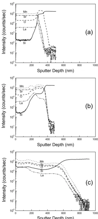
In order to precisely investigate the phase destruction of LSMO and the interreaction between the layers, TEM analyses with EDX and SIMS depth analysis were con- ducted on the samples annealed at 800
oC, 900
oC, and 950
oC, which corresponded to the samples of the single- phase LSMO, the unidentified-phase-included LSMO, and the phase-destroyed LSMO, respectively. Fig. 2 shows their cross-sectional TEM images and Fig. 3 presents their SIMS depth profiles. As can be seen in Fig. 2(a), when the LSMO film was annealed at 800
oC, a well-crystallized LSMO film was formed on the SiO
2underlayer, and the
distinct boundary between the layers was clearly shown.
The layer distinction could also be confirmed by the SIMS depth profile shown in Fig. 3(a), although some La accumulated at the interface between LSMO and SiO
2. However, in the image of the sample annealed at 900
oC shown in Fig. 2(b), a significant interdiffusion was ob- served. Notably, diffusion from LSMO to SiO
2appeared heavier than that in the reverse direction. The contrast of the SiO
2layer changed fully, and many bubbles appeared.
From the SIMS depth profile presented in Fig. 3(b),
Fig. 1. XRD patterns of the LSMO/SiO2 stacks annealed at varioustemperatures by using RTP.
Fig. 2. Cross-sectional TEM images of the LSMO/SiO2 stacks annealed at temperatures of (a) 800oC, (b) 900 oC and (c) 950oC by using RTP.
Fig. 3. SIMS depth profiles of the LSMO/SiO2 stacks annealed at temperatures of (a) 800oC, (b) 900oC and (c) 950oC by using RTP.
484 Ho-Jung Sun
significant diffusion of La, Sr, and Mn metal to the SiO
2layer was noticed, and the diffusion of these elements was also detected by TEM-EDX at point 2 in the middle of the SiO
2layer (Fig. 4(b)). The same EDX profiles as Fig.
4(b) were obtained in the areas of the bubbles which were not cross-sectioned because metal-diffused SiO
2was re- mained. The diffusion of Si from SiO
2to LSMO was also observed, but Si was not found everywhere in the layer.
The level of the SIMS Si profile in the upper part of the LSMO layer (Fig. 3(b)) was almost the same for the samples annealed at 800
oC (Fig. 3(a)). No Si was detected in the unreacted LSMO portion (point 1 in Fig. 2(b)), as presented in the TEM-EDX data in Fig. 4(a). The part of the LSMO near the interface, to which Si diffused, ap- peared amorphous, but the upper part still remained crys- talline. From the above results, it could be inferred that the diffusion of La, Sr, and Mn metal to SiO
2is faster than that of Si to LSMO. In Fig. 2(b), a thin layer in bright contrast was observed, which was determined to be unreacted SiO
2, as only Si and O were detected by TEM- EDX at point 3 (Fig. 4(c)). The Si-substrate that was far from the interreacted layer [point 4 in Fig. 2(b)] remained free of La, Sr, and Mn (Fig. 4(d)). When the annealing temperature was raised to 950
oC, full interdiffusion and interreaction occurred, and the intermixed layer became an amorphous one that contained expanded bubbles; this can be confirmed from the TEM image in Fig. 2(c) and the previously presented XRD pattern (Fig. 1).
It is believed that the La, Sr, and Mn metal atoms in LSMO diffuse into SiO
2more easily than Si atoms in SiO
2diffuse into LSMO, although the interdiffusion occurred simultaneously. La and Sr are known as network modifiers in fused silica,
11)thus the diffused metal atoms would break down Si-O bonds in fused silica. Moreover, a previous report on the synthesis of La
0.7Sr
0.3MnO
3/silca nanocom- posites suggested that Si-O-Si bonds in silica changed to Si-O-M (M = La, Sr and Mn) when the calcination tem- perature exceeded 800
oC based on micro-Fourier transform infrared spectroscopy analysis.
12)In fused silica, the loss of
connectivity results in greatly decreased viscosity. During the network modification by the metals in this work, some amount of Si would diffuse from SiO
2to LSMO. There- fore, some oxygen atoms lost bondage in the SiO
2glass network due to the resulting Si-deficiency, and so the debonded oxygen atoms must have been released as O
2gas. As the viscosity of the fused silica would decrease sig- nificantly, the released O
2gas could condense into bubbles.
Meanwhile, Si that diffused into LSMO changed the LSMO into the fused silica. When the annealing temperature was higher than that required for triggering interdiffusion above 800
oC, and when the annealing time was long enough, the above process of interdiffusion and interreaction would occur throughout the whole layers of LSMO and SiO
2, resulting in a metal-incorporated amorphous silicate layer with expanded bubbles.
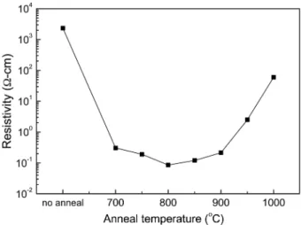
One of the best methods to investigate the interfacial reaction in this case was to evaluate the electrical property change of the LSMO film with respect to the variation of the annealing temperature. The room-temperature-resistivity of the LSMO film was examined, and the variation of the resistivity according to the annealing temperature is pres- ented in Fig. 5. As can be noticed from the figure, the resistivity of the as-deposited LSMO film dropped signifi- cantly by annealing at 700
oC, and the downturn continued up to 800
oC. However, the resistivity rebounded above 800
oC, and the resistivity increased steeply above 900
oC.
The resistivity variation of the LSMO was well congruent with the microstructural change discussed above. The re- sistivity decrease was related with the crystallization and the crystallinity enhancement of the LSMO film due to annealing, and the increase in resistivity above 800
oC was caused from the interreaction that changed the LSMO layer to the amorphous silicate form at the interface of LSMO/SiO
2.
Fig. 5. The variation of room-temperature-resistivity of the LSMO films according to the variation of the annealing temperature.
Fig. 4. TEM-EDX profiles analyzed from the LSMO/SiO2 stack an- nealed at a temperature of 900oC by using RTP. The spectra were taken at points (a) 1, (b) 2, (c) 3 and (d) 4, as designated in Fig. 2(b).
Thermal Instability of La0.6Sr0.4MnO3 Thin Films on Fused Silica 485
4. Conclusion
The interfacial reaction between LSMO and fused silica thin films by annealing was investigated. The LSMO film annealed at 800
oC exhibited good crystallinity, and the layer distinction against the underplayed SiO
2was well preserved.
However, when the annealing temperature was raised to 900
oC, interdiffusion and interreaction occurred. Most of the SiO
2and a part of the LSMO became amorphous silicate that incorporated La, Sr, and Mn and contained a lot of bubbles. At a higher temperature of 950
oC, the whole layer of LSMO and silica fully interdiffused, changing to an amorphous silicate layer that included the mixture of metals, in which the bubbles expanded. Therefore, in order to utilize La
1-xSr
xMnO
3thin films in Si-based integrated solid-state devices, the thermal instability of La
1-xSr
xMnO
3with the interlayer dielectric SiO
2should be considered carefully during thermal processing.
Acknowledgement
This study was supported by a grant from the Funda- mental R&D Program for Core Technology of Materials funded by the Ministry of Knowledge Economy, Republic of Korea.
References
1. M. B. Salamon and M. Jaime, Rev. Mod. Phys., 73, 583 (2001).
2. M. Bibles and A. Barthelemy, IEEE Trans. Electron Dev., 54, 1003 (2007).
3. A. -M. Haghiri-Gosnet and J. -P. Renard, J. Phys. Appl.
Phys., 36. R127 (2003).
4. J. Miao, X. G. Xu, Y. Jiang, L. X. Cao and B. R. Zhao, Appl. Phys. Lett., 95, 132905 (2009).
5. A. Huang, K. Yao and J. Wang, Thin Solid Films, 516, 5057 (2008).
6. S. Habouti, R. K. Shiva, C. -H. Solterbeck, M. Es-Souni and V. Zaporojtchenko, J. Appl. Phys., 102, 044113 (2007).
7. S. G. Choi, A. S. Reddy, B. -G. Yu, W. S. Yang, S. H.
Cheon and H. -H. Park, Thin Solid Films, 518, 4432 (2010).
8. P. K. Muduli, G. Singh, R. Sharma and R. C. Budhani, J.
Appl. Phys., 105, 113910 (2009).
9. Z. J. Wang, H. Usuki, T. Kumagai and H. Kokawa, J.
Cryst. Growth, 293, 68 (2006).
10. I. -B. Shim, C. -S. Kim, K. -T. Park and Y. -J. Oh, J. Magn.
Magn. Mater., 226-230, 1672 (2001).
11. Y. -M. Chiang, D. P. Birnie III and W. D. Kingery, Physical Ceramics: Principles for Ceramic Science and Engineering, p. 88, John Wiley & Sons, Inc., USA (1996).
12. Y. -H. Huang, C. -H. Yan, S. Wang, F. Luo, Z. -M. Wang, C. -S. Liao and G. -X. Xu, J. Mater. Chem., 11, 3296 (2001).
![Electrical and Magnetic Properties in [La0.7(Ca1-xSrx)0.3MnO3)]0.99/(BaTiO3)0.01 Composites](data:image/gif;base64,R0lGODlhAQABAIAAAP///wAAACH5BAEAAAAALAAAAAABAAEAAAICRAEAOw==)