Pt 촉매 박막을 이용한 비정질 SiO x 나노기둥의 수직성장
이지언1, 김기출2*
1
한국건설생활환경시험연구원 의료기기센터,
2목원대학교 신소재화학공학과
Vertical Growth of Amorphous SiO x Nano-Pillars by Pt Catalyst Films
Jee-Eon Lee
1, Ki-Chul Kim
2*1
Medical Device Evaluation Center, Korea Conformity Laboratories
2
Department of Advanced Chemical Engineering, Mokwon University
요 약 일차원 나노구조물은 양자 갇힘 효과 및 나노와이어가 갖는 체적 대비 높은 표면적 비에 기인하는 독특한 전기적, 광학적, 광전기적, 전기화학적 특성으로 인하여 많은 주목을 받아왔다. 특히 수직으로 성장된 나노와이어는 체적 대비 높은 표면적 비의 특성을 나타낸다. VLS(Vapor-Liquid-Soild) 공정은 나노구조물의 성장 과정에서 자기정렬 효과 때문에 더욱 주 목을 받는다. 본 연구에서는 두 영역 열화학 기상증착법을 이용하여 Si\SiO
2(300 nm)\Pt 기판 위에 수직으로 정렬된 실리콘 옥사이드 나노기둥을 VLS 공정으로 성장시켰다. 성장된 실리콘 옥사이드 나노기둥의 형상과 결정학적 특성을 주사전자현미 경 및 투과전자현미경으로 분석하였다. 그 결과 성장된 실리콘 옥사이드 나노기둥의 지름과 길이는 촉매 박막의 두께에 따라 변하였다. 실리콘 옥사이드 나노 기둥의 몸체는 비정질 상을 나타내었으며, Si과 O로 구성되어 있었다. 또한 성장된 실리콘 옥사이드 나노 기둥의 머리는 결정성을 나타내었으며, Si, O, Pt 및 Ti으로 구성되어 있었다. 실리콘 옥사이드 나노 기둥의 수직 정렬은 촉매물질인 Pt/Ti 합금의 결정성 정렬 선호에 기인하는 것으로 판단되며, 수직 성장된 실리콘 옥사이드 나노기둥 은 기능성 나노소재로 활용이 가능할 것으로 기대된다.
Abstract One-dimensional nanostructures have attracted increasing attention because of their unique electronic, optical, optoelectrical, and electrochemical properties on account of their large surface-to-volume ratio and quantum confinement effect. Vertically grown nanowires have a large surface-to-volume ratio. The vapor-liquid-solid (VLS) process has attracted considerable attention for its self-alignment capability during the growth of nanostructures. In this study, vertically aligned silicon oxide nano-pillars were grown on Si\SiO
2(300 nm)\Pt substrates using two-zone thermal chemical vapor deposition system via the VLS process. The morphology and crystallographic properties of the grown silicon oxide nano-pillars were investigated by field emission scanning electron microscopy and transmission electron microscopy. The diameter and length of the grown silicon oxide nano-pillars were found to be dependent on the catalyst films. The body of the silicon oxide nano-pillars exhibited an amorphous phase, which is consisted with Si and O. The head of the silicon oxide nano-pillars was a crystalline phase, which is consisted with Si, O, Pt, and Ti. The vertical alignment of the silicon oxide nano-pillars was attributed to the preferred crystalline orientation of the catalyst Pt/Ti alloy. The vertically aligned silicon oxide nano-pillars are expected to be applied as a functional nano-material.
Keywords : amorphous, catalyst film, nano-pillar, silicon oxide, vertical growth, VLS process
본 논문은 2017년도 과학기술정보통신부의 재원으로 한국연구재단의 지원을 받아 수행된 연구임(No. 2017R1A2B4012576)..
This work was supported by the National Research Foundation of Korea(NRF) grant funded by the Korea government(MIST, Ministry of Science and ICT) (No. 2017R1A3B4012576).
*
Corresponding Author : Ki-Chul Kim (Mokwon Univ.) Tel: +82-42-829-7489 email: [email protected]
Received October 10, 2017 Revised November 16, 2017
Accepted January 5, 2018 Published January 31, 2018
1. 서론
1차원 구조를 가지면서 높은 전기전도도와 인장강도 및 탄성률을 갖는 탄소나노튜브(Carbon NanoTube, CNT)가 발견된 이후 CNT에 관한 연구가 폭발적으로 진행되었다 [1]. CNT와 관련된 연구 열풍은 체적 대비 높은 표면적 비를 갖는 1차원 나노구조물인 Nanowires, Nanorods, Nanobelts 등으로 확대되었다. 다양한 방법으 로 Nanowires, Nanorods, Nanobelts 등을 합성하고, 이 들의 독특한 전기적, 광학적, 자기적, 광전기적 특징을 연구하여 응용하고자하는 많은 시도가 있었다. 특히 열 화학 기상 증착법(Thermal Chemical Vapor Deposition) 과 촉매 금속을 이용하는 Vapor -Liquid-Solid (VLS) 공 정으로 단결정 1차원 나노구조물을 합성하는 연구가 많 은 주목을 받았다. VLS 공정으로 합성되는 나노와이어 의 지름은 나노와이어 성장 초기에 핵성장에 관여하는 촉매 금속의 크기와 관련되며, 촉매 금속은 보통 물리기 상 증착법에 의한 박막 형태, 또는 금속 나노입자의 분산 을 이용한다. D. Gao 등은 Si(111) 기판 위에 Au를 촉매 로 사용하여 VLS공정으로 Si 나노와이어를 기판에 수직 으로(Vertically) 성장시켰고 [2], M. H. Huang 등은 사 파이어 기판 위에 Au를 촉매로 사용하여 VLS 공정으로 ZnO 나노와이어를 수직으로 성장시킨 후 385 nm 파장 의 자외선을 방출하는 나노레이저를 제조하였다[3]. 또 한 H-K. Park 등은 c-Al
2O
3/GaN/Au 기판 위에 ZnO 나 노와이어를 VLS 공정으로 수직 성장시켰다 [4]. ZnO 나 노와이어의 수직성장은 Thermal CVD를 이용한 VLS 공정뿐만 아니라 Solution Route로도 손쉽고 값싸게 성 장이 가능하였다 [5]. 1차원 나노와이어의 수직 성장은 이처럼 Si[2], ZnO[3-5], CNT[6, 7], Pd[8, 9] 등 다양한 소재에 대하여 많은 연구가 진행되었으며, 기능성 나노 소재의 성장과 관련된 중요한 연구주제이다.
반도체 나노와이어는 가스센서[9, 10], 태양전지[11], 광전소자[2, 12], 전계방출 트랜지스터[13, 14], 등 다양 한 응용분야에 활용될 수 있는 기능성 소재로서 체적 대 비 표면적이 높기 때문에 높은 반응성에 기초하여 기존 의 벌크 소재와는 다른 고기능성이 기대된다. 특히 1차 원 구조의 실리콘 나노와이어는 광전(Optoelectronic) 소 자 및 전기화학(Electrochemical) 소자로의 응용가능성 때문에 Galvanic Displacement 공정[2], 급속 열처리 공 정(Rapid Thermal Annealing)[15], 열증착(Thermal
Evaporation)[16]공정 등으로 실리콘 나노와이어를 성공 적으로 합성된 것이 보고되었다.
본 연구에서는 촉매 금속 Pt 박막과 Two-Zone Thermal CVD를 이용하여 VLS 공정으로 비정질 SiO
x나노와이어를 실리콘 웨이퍼 기판 위에 수직으로 성장시 켰다.
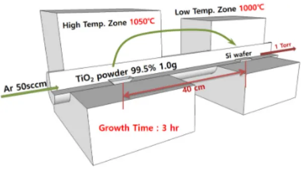
Fig. 1. Schematic diagram of vapor transport method for vertical growth of amorphous SiO
xnano-pillars by Pt catalyst films.
2. 실험방법
전형적인 열화학 기상 증착법이 변형된 Two-Zone
Thermal CVD를 이용하여 비정질 SiO
xNano-Pillar를
Si 기판 위에 수직으로 성장시켰다. 실험에 사용된 열화
학 기상 증착 장비는 Fig. 1에 나타낸 것처럼, 지름 2인
치의 Quartz Tube 내부에 지름 44 mm의 Inner Quartz
Tube가 구비되어 있어, Chamber의 오염을 방지하였고,
오염된 Chamber에 의한 영향도 배제하였다. Two-Zone
Thermal CVD는 Source와 기판부의 온도를 각각 제어
할 수 있는 2개의 히터가 구비되어 있어, 나노구조물이
성장되는 기판의 온도를 자유롭게 제어할 수 있다. 성장
실험을 진행하기 전에 로터리 펌프를 이용하여 Quartz
Tube 내부의 압력을 1 mTorr 이하로 유지하였고, Ar 가
스를 이용하여 수차례 Purging을 하였다. Silicon Oxide
나노와이어를 수직으로 성장시키기 위하여 Fig. 1에 나
타낸 것처럼, 알루미나 도가니에 순도 99.5%의 TiO
2파
우더를 1.0g 장착하고 1,050 ℃로 가열하였다. 기판은
아세톤, 에탄올, 탈이온수로 초음파 세척된 실리콘 기판
위에 스퍼터링 공정으로 촉매 금속 Pt 박막을 다양한 두
께로 증착하여 준비하였고, TiO
2Source로부터 40 cm
떨어진 곳에 기판을 위치시킨 후 히터를 1,000 ℃로 가
열하였다. 기화 된 Source를 운송하기 위한 Carrier Gas Ar을 50 sccm으로 흘려주었고, 이때 압력은 1.0 Torr였 다. 3시간 동안 실리콘 옥사이드 나노구조물을 성장시킨 후 히터를 상온으로 냉각시킨 다음 시료를 꺼내어 FE-SEM 및 TEM으로 morphology 및 결정학적 특성을 분석하였다.
3. 실험결과 및 고찰
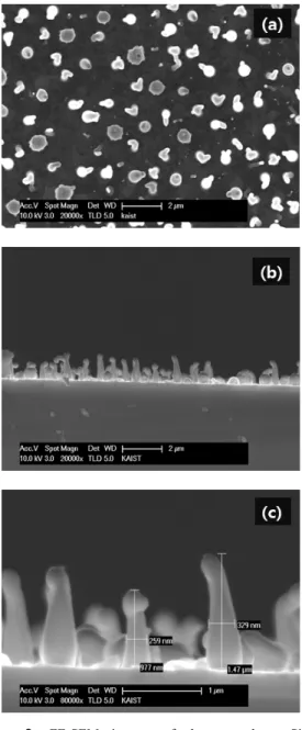
VLS 공정으로 성장된 나노와이어는 성장 초기에 핵 형성의 중심으로 작용하는 촉매 금속의 drop 크기에 의 존하여 나노 와이어의 지름이 결정되는 경향이 있다 [2-4]. 촉매 금속인 Pt 박막의 두께가 20 nm인 기판 위에 성장된 실리콘 옥사이드 Nano-Pillar의 주사전자현미경 분석 결과를 Fig. 2에 나타내었다. Fig. 2 (a)는 위에서 14
o기울어진 각도로 촬영한 이미지로서 실리콘 옥사이 드 나노와이어가 수직으로 성장된 모습을 관찰 할 수 있 다. Fig. 2 (b)에는 전자현미경의 Cross-Sectional 이미지 를 나타내었는데, Nano-Pillar의 지름은 약 200 ∼ 330 nm이었고, 길이는 약 500 nm 이었다. 지름이 50 nm 미 만인 실리콘 옥사이드 Nano-Pillar도 있었지만 대부분은 약 200 nm 내외의 굵기를 가지고 있었고, 길이는 약 500 nm로 비슷하였다.
Fig. 2. FE-SEM images of the amorphous SiO
xnano-pillars as grown on Pt catalyst film with 20 nm thickness, (a) tilted image (tilted angle is 14
o), (b) cross-sectional SEM image.
Fig. 3. FE-SEM images of the amorphous SiO
xnano-pillars as grown on Pt catalyst film with 40 nm thickness, (a) top view image, (b) cross-sectional SEM image, and (c) magnified cross-sectional SEM image.
촉매 금속의 두께 의존성을 조사하기 위하여 Pt 박막
의 두께를 40 nm로 증가시킨 기판을 사용하여 성장된
실리콘 옥사이드 나노구조물에 대한 주사전자현미경 분
석 결과를 Fig. 3에 나타내었다. 촉매 금속의 두께가 40
nm로 증가하였을 때 Nano-Pillar의 지름은 250 ∼330
nm 정도로 약간 증가하였으나, Nano-Pillar의 길이는
980 nm ∼ 1.5 μm로 두 배 이상 증가하였다. VLS 공정 으로 성장된 나노와이어의 길이는 보통 성장시간에 의존 하는 것이 일반적이지만[2], 본 연구에서는 성장시간을 6시간으로 증가시켜도 성장된 Nano-Pillar의 크기는 거 의 변하지 않았다. 즉 시간의존성은 나타나지 않았고, 오 직 촉매 금속의 두께에 의존하여 길이가 변하였다.
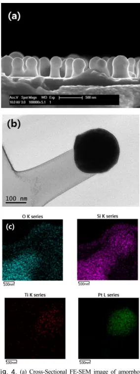
성장된 실리콘 옥사이드 Nano-Pillar의 Density가 낮 아서 XRD 분석이 불가능하였으므로, 결정학적 특성을 분석하기 위해 Focused Ion Beam(FIB) 공정으로 TEM 시료를 준비하였다. Fig. 4 (a)에는 촉매 금속 Pt 박막의 두께가 20 nm인 기판 위에 성장된 시료의 Cross-Sectional FE-SEM 이미지를 나타내었다. 비슷한 형태의 Nano-Pillar 중 가장 대표적인 Nano-Pillar를 Fig. 4 (b) 처럼 FIB 공정으로 분리하였고, Fig. 4 (c)에 나타낸 것 처럼 EDS(Energy Dispersive Spectroscopy) 분석을 실 시하여, Nano-Pillar의 구성성분을 분석하였다. 분석결과 Nano-Pillar의 몸체는 SiO
x인 것으로 분석되었으며, 머 리는 Si, O, Pt, 및 Ti의 성분이 공존하는 것으로 분석되 었다. 본 연구에 사용된 기판의 단면구조는 Si\SiO
2(300 nm)\Pt(20-40 nm)이었는데, 성장된 Nano-Pillar의 전체 에 걸쳐 나타나는 Si 성분은 기판에서 기인하는 것으로 판단된다[15]. O 성분은 TiO
2파우더 및 Si 기판의 절연 층(SiO
2)에서 기인하는 것으로 보이며, Nano -Pillar의 머리 부분에 존재하는 금속 성분 Pt와 Ti 성분은 촉매 박 막으로 사용된 Pt 박막과 Source 물질 TiO
2파우더에서 기인하는 것으로 판단된다.
Fig. 5에는 성장된 실리콘 옥사이드 Nano-Pillar의 머 리 및 본체 부분에 대한 HR-TEM 이미지 및 SAED(Selected Area Electron Diffraction) 패턴의 이미 지를 나타내었다. Fig. 5 (a)에 삽입된 SAED 패턴 분석 결과 성장된 Nano -Pillar의 머리 부분을 구성하고 있는 금속성분 Pt 및 Ti은 결정성을 가지고 있는 것으로 판단 된다. 하지만 Fig. 5 (b)의 HR-TEM 이미지 및 삽입된 SAED 패턴에서 볼 수 있는 것처럼 성장된 Nano-Pillar 의 몸체를 구성하고 있는 Si과 O는 비정질(Amorphous) 구조를 갖는 것으로 분석되었다.
Fig. 4. (a) Cross-Sectional FE-SEM image of amorphous SiO
xnano-pillars as grown on Pt catalyst film with 20 nm thickness. (b) TEM image of individual SiO
xnano-pillar fabricated by focused ion beam(FIB) process, (c) EDS mapping images of individual amorphous SiO
xnano-pillar fabricated by FIB process as shown
in (b).
Fig. 5. HR-TEM images of amorphous SiO
xnano-pillars of (a) head part and (b) body part of Fig. 4. (b).
The insets are selected area electron diffraction (SAED) patterns of red circle areas.
4. 결론
본 연구에서는 Thermal CVD를 이용하여 촉매 금속 Pt 박막과 Source 물질 TiO
2파우더를 이용하여 VLS 공 정으로 실리콘 옥사이드 나노와이어를 기판에 수직으로 성장시켰다. 성장된 실리콘 옥사이드 나노구조물의 Morphology와 결정학적 특성을 조사하였으며, 다음과 같은 결론을 내릴 수 있다.
1. 합성된 실리콘 옥사이드 나노구조물은 촉매 물질 Pt 박막과 Source 물질 TiO
2의 Ti 성분이 합금형 태로 나노구조물의 머리 부분을 형성하고 있으며, 결정학적 우선배향에 기인하여 VLS 공정으로 수 직성장한 것으로 판단된다.
2. 합성된 실리콘 옥사이드 나노구조물은 Amorphous 구조를 갖는 것으로 분석되었으며, 독특한 수직 성 장의 특성을 이용하여 기능성 나노소재로 활용이 가능할 것으로 기대된다.
References
[1] S. Iijima, “Helical microtubules of graphitic carbon”, Nature, Vol. 354, pp. 56-58, 1991.
DOI: https://doi.org/10.1038/354056a0
[2] D. Gao, R. He, C. Carraro, R. T. Howe, P. Yang, and R. Maboudian, “Selective Growth of Si Nanowire Arrays via Galvanic Displacement Processes in Water-in-Oil Microemulsions”, Journal of American Chemical Society, Vol. 127, pp. 4574-4575, 2005.
DOI: https://doi.org/10.1021/ja043645y
[3] M. H. Huang, S. Mao, H. Feick, H. Yan, Y. Wu, H.
Kind, E. Weber, R. Russo, and P. Yang,
“Room-Temperature Ultraviolet Nanowire Nanolasers”
Science, Vol. 292, pp. 1897-1899, 2001.
DOI: https://doi.org/10.1126/science.1060367
[4] H-K. Park, M. H. Oh, S-W. Kim, G-H. Kim, D-H.
Youn, S. Lee, S-H. Kim, K-C. Kim, and S-L. Maeng,
“Vertically Well-Aligned ZnO Nanowires on c-Al
2O
3and GaN Substrates by Au Catalyst”, ETRI Journal, Vol.
28, No. 6, pp. 787-789, 2006.
DOI: https://doi.org/10.4218/etrij.06.0206.0138
[5] C. H. Wang, A. S. W. Wong, and G. W. Ho, “Facile Solution Route to Vertically Aligned, Selective Growth of ZnO Nanostructures Arrays”, Langmuir, Vol. 23, pp.
11960-11963, 2007.
DOI: https://doi.org/10.1021/la702296q
[6] S. H. Lee, D. H. Lee, W. J. Lee, and S. O. Kim,
“Tailored Assembly of Carbon Nanotubes and Graphene”, Advanced Functional Materials, Vol. 21, pp.
1338-1354, 2011.
DOI: https://doi.org/10.1002/adfm.201002048
[7] H. Na, J. H. Park, J. Hwang, and J. Kim, “Site-specific growth and density control of carbon nanotubes by direct deposition of catalytic nanoparticles generated by spark discharge”, Nanoscale Research Letters, Vol. 8, p. 409, 2013.
DOI: https://doi.org/10.1186/1556-276X-8-409
[8] D. Xu, X. Yan, P. Diao, and P. Yin, “Electrodeposition of Vertically Aligned Palladium Nanoneedles and Their Application a Active Substrates for Surface-Enhanced Raman Scattering”, The Journal of Physical Chemistry, Vol. 118, pp. 9758-9768, 2014.
DOI: https://doi.org/10.1021/jp500667f
[9] J-S. Noh, J. M. Lee, and W. Lee, "Low-Dimensional Palladium Nanostructures for Fast and Reliable Hydrogen Gas Detection“, Sensors, Vol. 11, pp.
825-851, 2011.
DOI: https://doi.org/10.3390/s110100825
[10] L. Wang, Y. Kang, X. Liu, S. Zhang, W. Huang, and S.
Wang, “ZnO nanorod gas sensor for ethanol detection”, Sensors and Actuators B, Vol. 162, pp. 237-243, 2012.
DOI: https://doi.org/10.1016/j.snb.2011.12.073
[11] G. K. Mor, K. Shankar, M. Paulose, O. K. Varghese, and C. A. Grimes, “Use of Highly-Ordered TiO
2Nanotube Arrays in Dye-Sensitized Solar Cells”, Nano Letters, Vol. 6, No. 2, pp. 215-218, 2006.
DOI: https://doi.org/10.1021/nl052099j
[12] J-M. Wu, H. C. Shih, and W-T. Wu, “Formation and
photoluminescence of single-crystalline rutile TiO
2nanowires synthesized by thermal evaporation”, Nanotechnology, Vol. 17, pp. 105-109, 2006.
DOI: https://doi.org/10.1088/0957-4484/17/1/017 [13] J. Wu, Q. Gu, B. S. Guiton, N. P. de Leon, L. Ouyang,
and H. Park, “Strain-Induced Self Organization of Metal-Insulator Domain in Single-Crystalline VO
2nanobeams”, Nano Letters, Vol. 6, No. 10, pp.
2313-2317, 2006.
DOI: https://doi.org/10.1021/nl061831r
[14] L. Hongwei, L. Junpeng, Z. Minrui, T. S. Hai, S. C.
Haur, Z. Xinhai, and K. Lin, “Size effect on metal-insulator phase transition in individual vanadium dioxide nanowires”, Optic Express, Vol. 22, No. 25, pp.
30748-30755, 2014.
DOI: https://doi.org/10.1364/OE.22.030748
[15] Y-S. Lai, J-L. Wang, Z-C. Liou, and C-H. Tu,
“Tailoring of amorphous SiO
xnanowires grown by rapid thermal annealing” Chemical Physics Letters, Vol. 453, pp. 97-100, 2008.
DOI: https://doi.org/10.1016/j.cplett.2008.01.026 [16] Y. Shi, Q. Hu, H. Araki, H. Suzuki, H. Gao, W. Yang,
and T. Noda, “Long Si nanowires with millimeter-scale length by modified thermal evaporation from Si powder”, Applied Physics A, Vol. 80, pp. 1733-1736.
2005.
DOI: https://doi.org/10.1007/s00339-003-2469-x
이 지 언
(Jee-Eon Lee) [정회원]
•2016년 2월 : 목원대학교 신소재화 학공학과 (공학사)
•2017년 9월 : 한국건설생활환경시 험연구원 (연구원)
<관심분야>
바이오관련 나노소재, 에너지관련 소재, 기능성 나노소재
김 기 출