http://dx.doi.org/10.5369/JSST.2018.27.1.13 pISSN 1225-5475/eISSN 2093-7563
Synthesis of Nanoporous Metal Oxide Films Using Anodic Oxidation and Their Gas Sensing Properties
Jun Min Suh
1, Do Hong Kim
2, and Ho Won Jang
1,+Abstract
Gas sensors based on metal oxide semiconductors are used in numerous applications including monitoring indoor air quality and detecting harmful substances like volatile organic compounds. Nanostructures, for example, nanoparticles, nanotubes, nanodomes, and nanofibers have been widely utilized to improve gas sensing properties of metal oxide semiconductors, and this increases the effective surface area, resulting in participation of more target gas molecules in the surface reaction. In the recent times, 1-dimensional (1D) metal oxide nanostructures fabricated using anodic oxidation have attracted great attention due to their high surface-to-volume ratio with large- area uniformity, reproducibility, and capability of synthesis under ambient air and pressure, leading to cost-effectiveness. Here, we pro- vide a brief overview of 1D metal oxide nanostructures fabricated by anodic oxidation and their gas sensing properties. In addition, recent progress on thin film-based anodic oxidation for application in gas sensors is introduced.
Keywords: Gas sensor, Metal oxides, Anodic oxidation, Nanoporous, Nanotube
1. INTRODUCTION
The development of building structures and interior design for efficient and effective utilization of indoor space, has significantly increased the number of human beings spending their lives indoors. A recent survey on average Americans has revealed that they spend 93% of their lives indoors [1]. Therefore, the concept of indoor air quality has attracted a great deal of interest with regard to human health. Indoor air consists of ambient air and various minor gaseous substances emitted by various sources like building materials, printers, paints, glues, or even due to human activity. Those with a low vapor pressure, consequently existing in gaseous phase at room temperature, are classified as volatile organic compounds (VOCs). The VOCs, even in very small concentrations, are known for their potential harmful effects on the human body. For example, form aldehyde (HCHO) from
building materials induces sick building syndrome, while benzene (C
6H
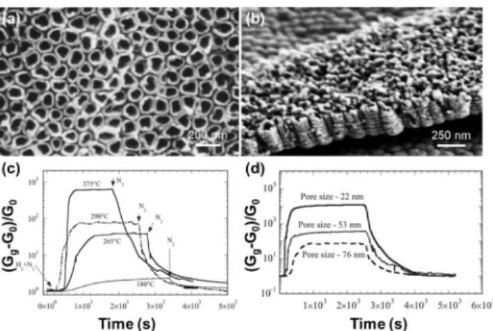
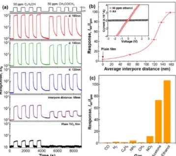
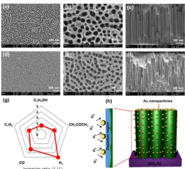
6) from car garages or tobacco smoke is notorious carcinogen [2,3]. In order to sensitively and selectively detect the VOCs and to prevent damages to human body, a lot of effort has been put into developing gas sensors with various materials. The gas sensors based on metal oxide semiconductors especially show very selective detection of VOCs, but their plain films show relatively low gas response. Since their low gas response can result in poor overall selectivity of various VOCs, a number of strategies including catalyst decoration [4-6], heterojunctions [7], and nanostructures [8-10] have been suggested to overcome the shortages. Metal oxide nanostructures in 1-dimension (1D), including nanorods, nanocolumns, nanotubes, or nanobamboos [11-16] have very high surface-to-volume ratio thus providing enlarged surface area to interact with the target gas molecules. The enlarged surface area contributes to an enhancement in the gas response, or sensitivity for the effective detection of the VOCs.
The 1D metal oxide nanostructures can be synthesized using various methods, such as dc sputter, e-beam evaporation, hydrothermal method, solvothermal method, etc. However, their synthesis conditions of high temperature and high pressure require complex and advanced equipment and long reaction times. As an alternative, anodic oxidation method, which is feasible at ambient air, temperature, and pressure with a high uniformity of the synthesized nanostructures, can be used.
Herein, we have summarized 1D metal oxide nanostructures
1
Department of Materials Science and Engineering, Research Institute of Advanced Materials, Seoul National Unversity
Gwanank-ro 1, Gwanak-gu, Seoul 08826, Republic of Korea
2
Department of Materials Science and Engineering, Korea University Inchon-ro 22 gil 6-3, Seongbuk-gu, Seoul 02841, Republic of Korea
+