Tin Sulphide Thin Films Formed by Sulphidising D.C.
Magnetron Sputtered Layers of Tin Using H
2S
M. Leach
†, D. Y. Jang
‡and R. Miles * Seoul National University of Science and Technology
* Northumbria University, Newcastle upon Tyne, UK
H
2S 가스를 이용한 황화주석 박막 증착에 관한 연구
마크리치†·장동영‡·로저 마일즈
*
서울과학기술대학교 국제융합학부 기계시스템디자인 (MSDE) 프로그램
*영국 노섬브리아대학교 전자 컴퓨터공학부
(Received September 30, 2010; Revised November 2, 2010; Accepted November 4, 2010)
논문초록 − 황화주석 박막을 만들기 위해 마그네트론 스퍼터 박막증착 공정을 통해 몰리브텐 유리 판위에 주석박막을 만들고 , 95% 알곤 +5% 황화수소 가스 혼합물을 사용하여 아닐링 공정을 통해 황화주석 박막을 형성하위에 증착하는것이 좋은 결과를 보여주고있다 . 박막면의 화학적 물리적 특
성을 전자현미경 , X 선 분석 , X 선회절을 통해 실험하였으며 , 아닐링 조건에 따른황화주석 박막의 파장대 반사율의 관계를 측정하였다 .
Abstract − Thin films of tin sulphide (SnS) have been formed by a novel 2-stage process where-in D.C. mag- netron sputtering was used to deposit to thin films of tin (Sn) and the layers then sulphidised using 5% hydrogen sulphide (H
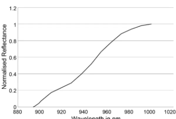
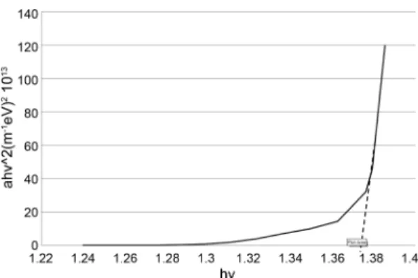
2S) gas in Argon. Although it was not found possible to deposit high quality thin films of tin directly onto glass substrates, excellent layers of tin were produced by using molybdenum (Mo) coated glass as the sub- strate material. The chemical and physical properties of the SnS layers formed were determined using scanning electron microscopy, energy dispersive x-ray analysis, x-ray diffraction studies and using reflectance versus wavelength measurements and these related to the conditions of synthesis. The data shows that it should be pos- sible to produce conventional “substrate structure” devices based on the use of this technology.
Keywords − 황화주석박막필름( tin sulphide thin films), 스퍼터링 (sputtering), 황화수소아닐링 (h
2s annealing), 물리적 특성 (physical properties)
1. Introduction
Thin film solar cells based on the use of cadmium tel- luride (CdTe) and copper gallium indium diselenide (CIGS) have been developed to lower the cost of manu- facture of photovoltaic cells and modules and these tech- nologies are now taking an increasing market share from
conventional silicon –based technologies[1]. However some problems remain. In the long term the lack of abundance of indium and gallium may limit the wide- spread use of CIGS technologies to generate power on a large scale. It is also desirable to make devices cadmium free, to satisfy environmental concerns. There are how- ever many other inorganic materials, which do not have these problems. In most cases their potential for use as PV materials has not been thoroughly assessed[2].
One such compound is SnS. Some of the important
†주저자
: [email protected]
‡책임저자