(Received March 22, 2011: Accepted April 25, 2011)
Abstract: Recently, board level solder joint reliability performance of IC packages during drop impact becomes a great concern to semiconductor and electronic product manufacturers. The handheld electronic products are prone to being dropped during their useful service life because of their size and weight. The IC packages are susceptible to solder joint failures, induced by a combination of printed circuit board (PCB) bending and mechanical shock during impact. The board level drop testing is an effective method to characterize the solder joint reliability performance of miniature handheld products. In this paper, applying the JEDEC (JESD22-B111) standard present a finite element modeling of the FBGA.
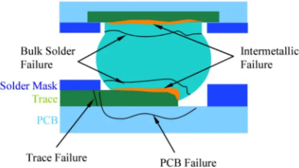
The simulation results revealed that maximum stress was located at the outermost solder ball in the PCB or IC package side, which consisted well with the location of crack initiation observed in the failure analysis after drop reliability tests.
Keywords: Board level drop test, Package drop test, Drop test
1. Introduction
The solder interconnection is one of the most important interconnection in IC packageing because it provides the mechanical and electrical interconnection between the package and the PCB. Solder joints connecting the IC package and PCB can be broken due to solder fatigue or bittle facture. Fatigue is caused by damage accumulation form temperature cycling or cycling bending, while brittle fracture is mainly caused by over stress due to extreme bending or drop impact. The mechanical shock resulted from mishandling during transportation or customer usage may cause solder joint failure of IC package, which leads to malfunction of product. Therefore, board level drop test is convenient evaluate the reliability of IC package in an accelerated test environment.
The JEDEC proposed board level drop test regulation to assess drop performance for surface mounted IC package.
1, 2)The board level drop test method is in widespread use for evaluating the drop reliability performance of IC package.
However this test needs large sample amount to show the distribution of reliability results, which means that the drop test is very expensive and time-consuming, requiring much manpower in measurement and failure analysis, it needs high cost. Therefore, simple and accurate simulations are necessary to develop the semiconductor package quickly.
In this study, we examine and computer simulation the board level drop test of package. FE analysis models were
established using ANSYS. And the input acceleration Input- G method is adopted to simulate the board level drop test by using ANSYS/LS-DYNA.
2. Theoretical Analysis
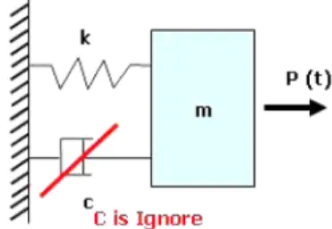
2.1. Single degree of freedom approach
For simplicity, the PCB assembly under drop impact can be treated as a single degree of freedom mass-spring-damping SDOF system. The governing equation of a one-degree of freedom linear dynamic system can be expressed as
(1)
where M, C and K are the system mass, damping coefficient and spring constant respectively, while x, and are the displacement, velocity and acceleration respectively, and P is force. But we assume that a spring-mass-undamped SDOF system (see Fig. 1).
Mx·· Cx· Kx + + = P
x· x··
†