플라즈마 표면처리 방법을 이용한
웨이퍼레벨 몰딩 공정용 기판의 최적 이형조건 도출
연 시 모⋅박 진 호⋅이 낙 규⋅박 석 희⋅이 혜 진
*한국생산기술연구원 마이크로나노공정그룹
Study on the Optimal Release Condition of Wafer Level Molding Process using Plasma Surface Treatment Method
Simo Yeon⋅Jeonho Park⋅Nukkyu Lee⋅Sukhee Park⋅Hyejin Lee*
Korea Institute of Industrial Technology, 143 Hanggaulro, Sangnok-gu, Ansan-si, Gyeonggi-do, 426-910, Republic of Korea
(Received 2015. 04. 14 / Accepted 2015. 05. 15)
Abstract : In wafer level molding progress, the thermal releasing failure phenomenon is shown up as the important problem. This phenomenon can cause the problem including the warpage, crack of the molded wafer. The thermal releasing failure is due to the insufficiency of adhesion strength degradation of the molding tape. To solve this problem, we studied experimental method increasing the release property of the molding tape through the plasma surface treatment on the wafer substrate. In this research, the vacuum plasma treatment system is used for release property improvement of the molding tape and controls the operating condition of the hydrophilic(O2, 100kW, 10min) and hydrophobic(C2F6, 200kW, 10min). In order to perform the peeling test for measuring the releasing force precisely, we remodel the micro scale material property evaluation system developed by Korea institute of industrial technology. In case of hydrophilic surface treatment on the wafer substrate, we can figure out the releasing property of molding tape increase. In order to grasp the effect that it reaches to the release property increase when repeating the hydrophilic treatment, we make an experiment with twice treatment and get the result to increase about 12%. We find out the hydrophilic surface treatment method using plasma can improve releasing property of molding tape in the wafer level molding process.
Key words : wafer level molding, plasma surface treatment, hydrophilic, hydrophobic, thermal release, peeling test
1. 서 론
1)IT 및 반도체 산업 등의 급격한 발전에 힘입어 최근 의 첨단 전자, 통신제품은 초 경량화, 초 소형화, 고기 능복합화 기반의 하이엔드(High-end)급 제품성능의 구현이 필수적이다. 고성능 전자제품 구현을 위한 반 도체분야의 기술개발은 제조공정 전 분야에서 활발히 진행되고 있으며, 2차원(2D) 및 3차원(3D) 패키지 기 반의 집적도 향상에서 패키징 기술개발 분야로 패러
*Corresponding author, E-mail: [email protected]
다임의 변화가 진행되고 있다. 3차원(3D) FOWLP(Fan Out Wafer Level Package) 기술은 고성능․초박형 반도 체 구현에 있어 차세대 제품 구현을 위한 차세대 패키 지기술이며, 제조비용의 절감과 함께 우수한 패키지 성능(전기적, 열적, 신뢰성 확보)을 가능케 하는 핵심 기술로 연구되어지고 있다. FOWLP 기술은 패키지 범 프가 실리콘 칩 외부 영역까지 존재함에 따라 패키징 확장성과 입출력의 증가가 가능한 패드 확장(Fan-out) 의 장점을 유지하고 웨이퍼 레벨의 패키징을 가능케 하는 기술로 아래와 같은 특징을 가지고 있다.1)-14)
▪ 3차원 패키지를 통하여, 기존 실리콘(Si) 기술연장, 디 바이스 사이즈 축소, 배선 RC 지연(RC : Resistance․
Capacitance Delay) 저감 등 성능 향상 및 높은 집적도 의 구현이 가능함
▪ 유연한 공정조합이 가능함에 따라 융합형 시스템 반 도체의 구현을 가능케 함
▪ 고성능 반도체 생산의 제조비용 절감이 가능한 미 래 패키지 공정기술임
Fig. 1 3D Semiconductor Packaging(Pop, SiP)
본 논문에서는 3차원(3D) FOWLP(Fan Out Wafer Level Package) 공정에서 대구경 웨이퍼에 실장된 반 도체칩의 신뢰성 향상 및 표면을 Compound로 패키징 하기 위한 가압몰딩공정 중 몰딩된 웨이퍼기판 (Substrate)과 몰딩테이프(Molding Tape)를 제품에 손 상이 가지 않고 박리하기 위한 최적화 공정조건을 형 성하기 위한 방법을 적용한다. 그리고 이에 대한 적용 가능성 확인을 위한 실험적 연구 결과에 대해 제시하 였다.
2. 대구경 웨이퍼 레벨 가압몰딩공정
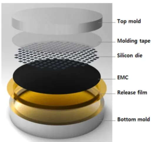
대구경 웨이퍼 레벨 가압몰딩공정은 대구경 웨이 퍼에 실장된 반도체칩의 외부로부터의 물리적, 화학 적 충격 방지 및 외부의 습기나 불순물로부터 보호할 수 있도록 EMC(Epoxy Molding Compound, 수지의 일 종)로 밀봉 성형하는 공정이다. 반도체칩이 실장된 대 구경 웨이퍼의 표면을 패키징하기 위한 공정(Surface Molding)은 Fig. 2와 같이 상하금형, 실장된 반도체칩 을 부착한 몰딩테이프와 EMC 분리를 위한 이형필름 (Release Film)으로 구성된다. 또한 전후공정의 연계
Fig. 2 Compression molding components
및 패키지의 원활한 이동을 위한 기판(Substrate)위에 몰딩테이프를 부착하여 가압몰딩공정(Compression Molding Process)을 수행한다.
(a) System layout drawing
(b) Compression molding module Fig. 3 W/L Compression molding system
3. 문제도출 및 해결방안 제시
몰딩 테이프는 몰딩공정 중 웨이퍼기판과 다이 간 에 점착력을 가지고 실리콘 다이의 정렬을 유지하여 후 공정에서 설계된 공정을 수행할 수 있도록 하는 기 능을 가진다. 몰딩 공정 후 성형된 웨이퍼(Molded wafer)를 웨이퍼기판으로부터 박리하기 위해 열박리 이형 테이프를 사용하고 있다. 몰딩 테이프의 베이스 필름의 한 면은 압력반응 접착기능을 가지고 있으며, 다른 면의 접착소재 내부에 열발포 기능을 가지는 캡 슐이 포함되어 가열공정을 통해 캡슐이 팽창하면서 이형이 되게 한다.
웨이퍼 레벨 몰딩공정에서 주요 공정불량 중 하나 는 몰딩 후 열박리 불량 현상으로, 성형된 웨이퍼의 변 형(Warpage), 파단(Crack) 등의 문제요인을 유발한다.
이러한 열박리 불량은 몰딩 후 몰딩테이프의 이형 접 착력 저하 미흡으로 인해 발생되며, 본 연구에서는 이 를 해결하기 위한 방안으로 웨이퍼기판의 플라즈마 표면처리를 통하여 몰딩 테이프의 이형성을 간접적으 로 증가시키는 방법을 적용하여 이러한 문제요인을 최소화하는 방법에 대해 실험적으로 연구하였다.
(a) Molded wafer (Before molding tape release)
(b) Molded wafer (After molding tape release) Fig. 4 Molded wafers with release problem
4. 최적 이형조건 도출 실험
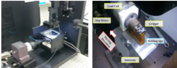
몰딩 테이프의 이형성 향상을 위한 플라즈마 표면 처리는 진공 플라즈마 장비(Europlasma, CD400MC)를 사용하였고, 친수성 코팅은 O2, 100 kW 분위기에서 소 수성 코팅은 C2F6, 200 kW 분위기에서 각각 10분간 처 리하였다. 이후 웨이퍼기판에 몰딩 테이프(10×140 mm2)를 접착하고 170 ℃ 온도조건에서 열발포 공정을 수행하였다. 이형성 평가를 위한 필링(Peeling) 테스트 는 한국생산기술연구원에서 개발한 마이크로물성평 가시스템을 정밀한 하중특성을 측정할 수 있도록 개 조하였고, 본 시스템을 이용하여 0.5 mm/s의 속도로 몰딩테이프가 박리될 때의 하중을 측정하였다.
Fig. 5 Modified peeling test system (KITECH)
(a) Peeling test specimen (size : 10×140 mm2)
(b) Plasma treatment and Thermal release process Fig. 6 Specimens of Release property testing
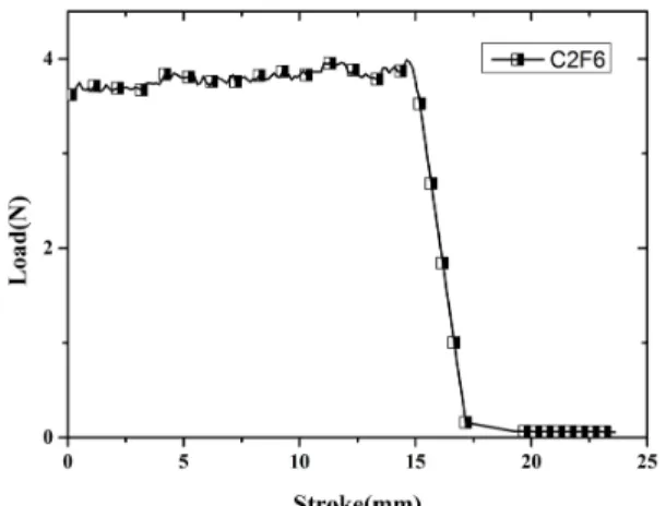
Fig. 7 Data plotting chart of peeling test results Table 1 Release property testing results
(peeling test, Unit : N) 2nd layer treat
No-Treat Hydrophilic Hydrophobic
1st layer treat
No-Treat 3.80 3.69 3.78
Hydrophilic 3.69 3.38 3.76
Hydrophobic 3.78 3.66 3.79
실험결과 웨이퍼기판에 친수성 플라즈마 표면처리 를 하였을 때 몰딩 테이프 이형성이 증가하는 것으로 나타났으며, 반복 처리를 통한 이형성 증가를 검증하 기 위해 2회 반복실험을 매트릭스 조건으로 수행한 결 과 플라즈마 친수 표면처리를 반복할수록 이형성이 지속적으로 향상되는 것을 파악할 수 있었다.
5. 결 론
대구경 웨이퍼 레벨 패키징 공정에서 제품 표면을 복합소재(EMC)로 패키징하는 가압몰딩공정에서 몰 딩된 웨이퍼기판(Substrate)과 몰딩 테이프(Molding Tape)를 제품에 손상이 가지 않고 박리하기 위한 최적 화 공정조건을 도출하기 하기 위해 플라즈마 표면처 리 방법을 적용하였다.
실험적 연구를 통해 웨이퍼기판의 표면을 친수처 리를 하는 경우에 몰딩 테이프 이형성이 증가하는 것 을 파악할 수 있었으며, 2회 반복 처리를 할 경우 그 효 과가 약 12%정도 향상되는 것을 파악하였다. 본 연구 를 통해 웨이퍼 레벨 몰딩공정에서 웨이퍼 기판 표면
을 플라즈마 친수 처리함으로써 열박리 불량현상을 개선할 수 있음을 확인하였다.
Acknowledgement
본 연구는 산업통상자원부에서 지원한 “300mm 대 응 대구경 다층구조의 복합 패키지 공정 및 장비 기술 개발”과제(Grant No. 10041083)를 통해 수행되었습니 다. 이에 관계자 여러분께 감사드립니다.
References
1) M. Brunnbauer, E. Furget, G. Beer, T. Meyer,
“Embeddedd wafer level ball grid array (eWLB)”, Electron. Packag. Technol. Conf., p. 1~5, 2006.
2) P. Sun, V. Leung, D. Yang, R. Lou, D. Shi, T. Chung,
“Development of a new Packge-On-Package(POP) structure for next-generation portable electronics”, Electron. Compo. and Technol. Conf., p. 1957~1963, 2010.
3) M. Dreiza, J. S. Kim, L. Smith, “Joint project for mechanical qualification of next generation high density Package-On-Package(POP) with through mold via technology”, Microelectron. and Packag.
Conf., p. 1~8, 2009.
4) Yole development, “Embedded wafer level packages:
Fan out WLP/ Chip embedding in substrate”, 2010.
5) R. Fillion, C. Woychick, T. Zhang, D. Bitting,
“Embedded chip build-up using fine line Interconnect”, Electron. Compo. and Technol. Conf., p. 49~53, 2007.
7) A. Ostmann, D. Manessis, T. Loeher, A. Neumann, H.
Reichl, “Strategies for embedded of active components”, Intl. Microsystems, Packag., Assembly Conf. Taiwan, p.
1~4, 2006.
8) P. Palm, J. Moisala, A. Kivikero, R. Tuominen, A.
Iihola, “Embedding active components inside printed circuit board(PCB) a solution for miniaturization of electronics”, Advanced Packag. Materials: Processes, Properties and Interfaces, 2005 Intl. Symposium on Digital Object Identifier, p. 1~4, 2005.
9) M. J. Yim, R. Strode, J. Brand, R. Adimula, J. J.
Zhang, C. Yoo, “Ultra thin POP top package using compression mold: Its warpage control”, Electron.
Compo. and Technol. Conf., p. 1141~1146, 2011.
10) C. H. Khong, A. Kumar, X. Zhang, G. Sharma, S. R.
Vempati, K. Vaidyanathan, J. H. -S. Lau, D. L.
Kwong, “A novel method to predict die shift during compression molding in embedded wafer level package”, Electron Compo. and Tech. Conf., p.
535~541, 2009.
11) L. Ji, D. V. Sorono, T. C. Chai, X. Zhang, “3-D numerical and experimental investigations on compression molding in multichip embedded wafer level packaging”, Packag. and Manuf. Technol., Vol.
3, Issue 4, p. 678~687, 2012.
12) L. Ji, H. J. Kim, F. Che, S. Gao, D. Pinjala,
“Numerical study of preventing flow-induced die-shift in the compression molding for embedded wafer level packaging”, Electron. Packag. Technol. Conf., p.
406~411, 2011.
13) G. Sharma, A. Kumar, V. S. Rao, S. W. Ho, V.
Kripesh, “Solution strategies for die shift problem in wafer level compression molding”, Packag. and Manuf. Technol., Vol. 1, Issue 4, p. 502~509, 2011.
14) N. W. Pascarella, D. F. Baldwin, “Compression flow molding of underfill encapsulats for low cost flip chip assembly”, Electron Compo. and Tech. Conf., p.463~470, 1998.