Ⅰ. Introduction
The throughput rate of digital signal processing systems operating on analog inputs is often limited b the speed of the analog-to–digital
* 이 논문은 2017년도 정부(과학기술정보통신부)의 재원으로 정보통신 기술진흥센터의 지원을 받아 수행된 연구임 (No. 2017-0-00274, 다중 채널 TI ADC에서 미스매치에 대한 디지털 후면 교정 기술 개발)
** 조선대학교 정보통신공학과 박사과정
*** 조선대학교 정보통신공학과 교수(교신저자)
interface. To increase the speed beyond the technological limit, the A/D interface can consist of more than one component ADC interleaved in time. The main problem with TI ADCs is that linear errors in the constituent channels, which do not affect their linearity, give rise to nonlinear errors in the TI ADC output when there are asymmetries among the channels.
In TI ADC, different mismatch noise can cause the output signal to distort which is the sum of
TI ADC를 위한 시간 왜곡 교정 블록의 하드웨어 구현
*칸 사데크 레자**ㆍ최 광 석***
Hardware Implementation of Time Skew Calibration Block for Time Interleaved ADC
Khan Sadeque Reza ․ Choi Goangseog
<Abstract>
This paper presents hardware implementation of background timing-skew calibration technique for time-interleaved analog-to-digital converters (TI ADCs). The timing skew between any two adjacent analog–digital (A/D) channels is detected by using pure digital Finite Impulse Response (FIR) delay filter. This paper includes hardware architecture of the system, main units and small sub-blocks along with control logic circuits. Moreover, timing diagrams of logic simulations using ModelSim are provided and discussed for further understanding about simulations. Simulation process in MATLAB and Verilog is also included and provided with basic settings need to be done. For hardware implementation it not practical to work with all samples. Hence, the simulation is conducted on 512 TI ADC output samples which are stored in the buffer simultaneously and the correction arithmetic is done on those samples according to the time skew algorithm. Through the simulated results, we verified the implemented hardware is working well.
Key Words : Time Interleaved Analog-to-digital Converter (TI ADC), Digital Calibration, Timing Error, Finite Impulse Response (FIR), MATLAB
spurious tones and aliased versions of the input signal. Those mismatches significantly reduce the Signal-to-Noise and Distortion Ration (SNDR) and the Spurious Free Dynamic Range (SFDR) of the converter[1-3]. So an entirely digital method of TI ADC time skew error calibration is presented in this paper[4-6]. The calibration process is implemented in three spheres of mismatches, offset mismatch, gain mismatch and time skew mismatch[7-9]. The calibration algorithm is mainly based on statistical properties of signals for error estimations, particularly targeting mean and variance of samples[10]. This work focus only on the hardware implementation of the time skew calibration method for TI ADC.
This paper illustrates the hardware implementation for the time skew calibration for TI ADC. In contrast with offset and gain calibration, the time skew calibration is performed by using pure digital FIR delay filter [5, 6, 8, 9]. Before time skew calibration the gain corrected samples are also refined using a smoothing block. The smoothing operation is also based on the mean value calculation.
Hardware implementation of high speed applications is always challenging because of throughput and chances of timing violations. The concepts of parallelism and pipelining are adapted in implementation phase in order to meet high speed requirements. As proposed algorithm indicates the complexity in terms of high data line widths due to statistical parameters computations, thus, the use of registers in iterative computations make it tricky in
register-transfer level (RTL). Overall design of digital calibration consists of four primary units;
offset calibration, gain calibration, smoothening block and time calibration. Adders, subtractors, multipliers and dividers are the key computational units along with small control units of some individual modules. Further, memory components are the key units for high speed digital signal processing algorithms and plays important role in minimizing the resources of design.
The design proposed in this paper is implemented in Verilog HDL and written in synthesizable format. Testing of system proved the functionality of system by matching the outputs with actual algorithm implemented in fixed point MATLAB. In addition, as the data samples cannot be provided to any hardware unit, hence unit of 512 samples is processed sequentially by the system meanwhile storing the coming samples into buffer and processing after in units of 512 samples every time. Testing vectors are generated through MATLAB algorithm for input to the RTL and at the end output of Verilog and MATLAB fixed point are compared. The results stated that the degradation of performance occurs as it always do in hardware because of several reasons; such as, hardware cannot take all the data samples on same time as MATLAB simulations. Moreover, precision factor has its own impacts on degradations of performance in hardware whereas in MATLAB simulations, precision is not a concern. To verify the performance designed
system is synthesized in order to make sure that timing violations do not exist. Design Compiler, Synopsys EDA tool, is used for synthesis with 130㎛ CMOS libraries. Synthesis results suggest that the timing violations did not occur.
Section 2 describes the overall top module of the digital calibration block. Section 3 and 4 illustrates the hardware design methodology for time skew calibration block. Section 5 describes the timing diagram and finally section 6 concludes the paper.
Ⅱ. Digital Calibration Hardware Architecture
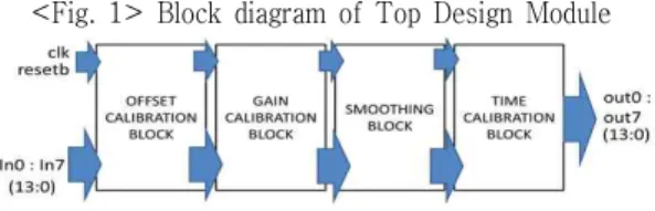
The overall hardware design of digital calibration consists of four hardware units; offset calibration, gain calibration, smoothening and time calibration. These blocks are divided into further small units for design simplicity. Eight channel inputs, each of twelve bits, provided to digital calibration block as input along with 2.6㎱
clock signal and Asynchronous active low reset.
Moreover, the system will produce eight outputs of respective channel, each of 14 bits from the time calibration block. The overall system throughput is 384 MS/s as per the requirements.
Figure 1 shows the block level hardware
architecture of the system and in RTL, it is expressing TOP module. The focus of this paper is limited to time calibration block.
Ⅲ. Time Calibration Block
3.1 Time Calibration Block Top Entity
Figure 2 is the top entity of time skew calibration block. The inputs of this block are coming from the top entity of smoothening block.
The 13-bit inputs smth_out0 to smth_out7 are the corrected output from the smoothening top entity and the wr_enable is 1-bit input which notify the top time calibration entity that from which point the input buffer of time calibration block will start storing the smoothing corrected outputs. The two other inputs are the clk and the resetb. Eight 14-bit output (OUTPUT1 to OUTPUT8) are coming out from the top module of time calibration block. The outputs are unsigned and fed to the unsigned to 2’s complement converter block
3.2 Time Calibration Block Input Buffer Module
Figure 3 shows the input buffer module of the time calibration block. If the enable signal is present at the input then the input buffer will start to store data coming from the smoothing block. With the increment of write pointer eight data will be stored in the input buffer
<Fig. 1> Block diagram of Top Design Module
consecutively and the data will be serially fetched till the end slot of the input buffer.
<Fig. 2> Time Calibration Block Top Entity
<Fig. 3> Time Calibration Block Input Buffer Module
Buffer length is 512 and width is 13 bits. After starting increment when the write pointer reaches at eight, it enables the Read Enable1 signal which results the buf_out0 output to the filter module. The bypass_en8 signal and the bypass8 output are also forwarded to the filter module at the same time. The purpose of the bypass_en and bypass signals are to replace the first value
of the filter with proper value as the first value of the filter is always distorted because of the delay present in the filter module. In the same manner when the write pointer is at 72,136, 200, 264, 328, 392 and 456, the input buffer module transfers the buffer1 to buffer 7 data, Read Enable, bypass_enable, bypass signals to the corresponding filters, respectively.
<Fig. 4> Filter Module of Time Calibration Block
<Fig. 5> Time Calibration Block Output Buffer Module
3.3 Time Calibration Block Filter Module
Figure 4 shows the filter module of time calibration block. Filter module is a first order FIR low pass filter and it includes 8 filters. The input of the filter is coming from input buffer module and it is pipelined. Filter input is the thirteen bit input buffer output (buf_out0 to buf_out7). FIR filter coefficient is 0.5. In the filter module, the input signal is fetched to the filter coefficient multiplier and also to the delay (D-flip flop). After the delay the input is again multiplied with the filter coefficient. But this part is multiplexed with the thirteen bit bypass signal and controlled by bypass_en signal. As the first output of filter is distorted, so the bypass and bypass_en signals are used to correct the first output of the filter. Before sending to adder module the coefficient multiplied signals are pipelined again. To generate appropriate output the filtered signals are multiplied with a constant value (1.03125) and to avoid timing mismatch the filter output is also pipelined. The final filter output is 14-bit (fout1 to fout8). This output is fed to the output buffer module along with an enable signal (buf_en) as shown in Figure 5. Each filter generates a buffer enable signal, buf1_en to buf8_en respectively, according to the filter output present.
3.4 Time Calibration Block Output Buffer Module
Figure 5 shows the architecture of output buffer
module for time calibration block. The length of the output buffer is 512 and the width is 14 bit.
Output buffer starts storing the data coming from the filter module when it receives the buffer enable signal. The signals buf0_en to buf7_en are for the buffer block 0 to 7 respectively. When buffer enable signals (buf0_en to buf7_en) are present, the output buffer write pointer (Write Pointer0 to Write Pointer7) starts to increment and also buffer starts to store the of filter output (fout1 to fout7). In this output buffer module, the data are stored serially. With the write pointer another counter, write counter starts to count the number of data stored in the buffer. When Write Counter7 reaches 7, the output buffer starts to supply output. Eight outputs are available form output buffer in every clock cycle and it starts from Buffer0. The output is controlled by using read counter which increments by eight in every clock cycle and it provides eight output serially in from Buffer0 to Buffer7.
Ⅳ. Unsinged to 2’s Complement Converter
The overall processing of digital calibration block is done on the unsigned data. So there is an unsigned to two’s conversion module is added in the output of the digital calibration block as shown in figure 6. The 14-bit final output (out0 to out7) is in two’s complement format by default. If the select_unsign signal is 1 then the module will provide unsigned output.
Ⅴ. Timing Diagrams
Figure 7 shows the time diagram of time calibration block input buffer module and it shows the signals of Buffer0. When the thirteen
bit data (buf_in0 to buf_in7) and write enable signal (enable) is present from smoothening module, the write pointer (wr_ptr) starts incrementing by eight and the input buffer stores eight data and it continues till the last position of Figure 7: Timing Diagram of Time Calibration Block Input Buffer Module (Buffer0)
Figure 8: Timing Diagram of Time Calibration Block Output Buffer Module (Buffer0)
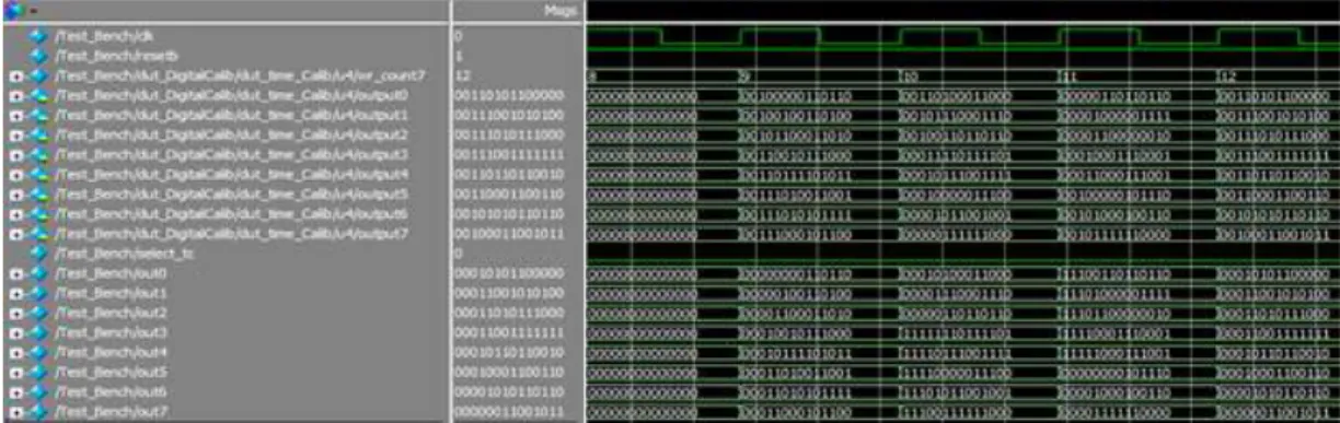
Figure 9: Timing Diagram of Unsigned to Two’s Complement Converter Output
input buffer. In every clock cycle the buffer memory stores eight data and the process is serial. At write pointer (wr_ptr) is incremented by eight the read enable signal (rd_en0) is 1 and the buffer provides output with the increment of read pointer (rd_prt0). Simultaneously the bypass_en is high and the bypass is 0.
Figure 8 shows the timing diagram of output buffer module of time calibration block. When the buffer enable signal (buf0_en) is high Buffer0 starts storing data according to input (buf_in0) that is the filter output(fout1) with the increment of write pointer0. Similarly, when the second buffer enable signal (buf1_en) is present, Buffer1 stores input (buf_in1) data.
Figure 9 shows the timing diagram of unsigned to two’s complement converter module output. When the write pointer counter, wr_count7 exceeds 7 the output buffer of time calibration block starts providing eight, fourteen bit unsigned output and the unsigned to two’s complement converter converts the unsigned output to two’s complement output when the select pin select_tc is zero by default.
Ⅵ. Conclusion
Hardware implementation of purely digital method for timing calibration of TI ADC is approached in this paper. Algorithm is developed by combining on statistical method and digital filter method. Hardware development is completed based on the developed algorithm and
the simulation output is matched for both MATLAB and Verilog. It is impractical for a real time system to work with such extensive number of samples. So for hardware implementation a constant range of samples are selected for processing. After comparing the output of this system with some other hardware implemented calibration system it can be concluded that it is producing quite satisfactory result. The hardware is implemented and tested for large number of test vectors and the expected output is achieved successfully.
참고문헌
[1] M. E. Chammas and B. Murmann, “A 12 GS/s 81-mW 5-bit time-interleaved flash ADC with background timing skew calibration,”
IEEE Journal of Solid–State Circuits, Vol. 48, No. 7, 2011, pp. 838-847.
[2] F. Centurelli, P. Monsurro, and A. Trifiletti,
“Efficient digital background calibration of time-interleaved pipeline analog-to-digital converters,” IEEE Transactions on Circuits and Systems I: Regular Papers, Vol. 59, No. 7, 2012, pp. 1373-1383.
[3] F. Centurelli, and P. Monsurro, “Improved digital background calibration of time-interleaved pipeline A/D Converters,”
IEEE Transactions on Circuits and System II:
Express Briefs, Vol. 60, No. 2, 2013, pp. 86-90.
[4] V. Divi, and G. Wornell, “Blind calibration of timing skew in time-interleaved analog-to -digital
converters,” IEEE Journal of Selected Topics in Signal Processing, Vol.3, No.3, 2009, pp.
509-522.
[5] A. Haftbaradaran, and K.W. Martin, “A background sample-time error calibration technique using random data for wide-band high-resolution time-interleaved ADCs,” IEEE Transactions on Circuits and System II:
Express Briefs, Vol. 55, No. 3, 2008, pp.
234-238.
[6] S. Huang, and B.C. Levy, “Blind calibration of timing offsets for four-channel time-interleaved ADCs,” IEEE Transactions on Circuits and System I: Regular Papers, Vol.54, No. 4, 2007, pp. 863-876.
[7] Y.C. Jenq, “Digital spectra of non-uniformly sampled signals: fundamentals and high-speed waveform digitizer,” IEEE Transactions on Instrumentation and Measurement, Vol. 37, No. 3, 1988, pp. 245-251.
[8] H. Johansson, and P. Lowenborg,
“Reconstruction of non-uniformly sampled band-limited signals by means of digital fractional delay filters,” IEEE Transactions on Signal Processing, Vol. 50, No. 11, 2002, pp.
2757-2767.
[9] S. M. Jamal, D. Fu, M.P. Singh, P.J. Hurst, and S.H. Lewis, “Calibration of sample-time error in a two-channel time-interleaved analog-to- digital converter,” IEEE Transactions on . Circuits and Systems I: Fundamental Theory
and Applications, Vol. 51, No. 1, 2004, pp.
130-139.
[10] S.M. Jamal, D. Fu, N.C.-J. Chang, P.J. Hurst, and S.H. Lewis, “A 10-b 120-Msample/s time -interleaved analog-to-digital converter with digital background calibration,” IEEE Journal of Solid–State Circuits, Vol. 37, No. 12, 2002, pp. 1618-1627.
▪저자소개▪
칸 사데크 레자 (Khan Sadeque Reza)
2015년 3월~현재 조선대학교 정보통신공학과 박사과정
2014년 6월 National Institute of Technology, Karnataka (인도) VLSI Design 전공(공학석사)
2010년 12월 University of Liberal Arts Bangladesh (방글라데시) 통신공학과(공학사)
관심분야 : 이식형 생체신호처리 및 방송정보통신 신호처리 VLSI 설계 E-mail : [email protected]
최 광 석 (Choi Goangseog)
2006년 3월~현재
조선대학교 정보통신공학과 교수 2002년 2월 고려대학교 전자공학과(공학박사) 1989년 2월 부산대학교 전자공학과(공학석사) 1987년 2월 부산대학교 전자공학과(공학사)
관심분야 : 방송정보통신 및 이식형 생체신호처리 SoC 설계 E-mail : [email protected]
논문접수일 : 수 정 일 : 게재확정일 :
2017년 08월 06일 2017년 08월 24일 2017년 08월 29일