DOI:10.5369/JSST. 2011.20.3.162 pISSN 1225-5475/eISSN 2093-7563
Light-Adaptive Vision System for Remote Surveillance Using an Edge Detection Vision Chip
Kyung-Hwa Choi1, Sung-Hyun Jo2, Sang-Ho Seo3, and Jang-Kyoo Shin2,+
Abstract
In this paper, we propose a vision system using a field programmable gate array(FPGA) and a smart vision chip. The output of the vision chip is varied by illumination conditions. This chip is suitable as a surveillance system in a dynamic environment. However, because the output swing of a smart vision chip is too small to definitely confirm the warning signal with the FPGA, a modification was needed for a reliable signal. The proposed system is based on a transmission control protocol/internet protocol(TCP/IP) that enables monitoring from a remote place. The warning signal indicates that some objects are too near.
Keywords : FPGA, Edge detection, Remote surveillance, Vision chip.
1. INTRODUCTION
Vision systems have many applications and are used in military surveillance, unmanned parking lots for the disabled, robotic eyes, and closed circuit television (CCTV). A vision system is required for selectivity in determining an object's movement, because of the large quantity of image data that must be processed. Therefore, the edge signal obtained from the object must be used efficiently.
Generally, surveillance systems use a charge coupled device(CCD) camera for image acquisition and then confirm the image after signal processing through peripheral circuits. These systems are not only sensitive to variations of background illumination, but also have many problems including non real-time processing due to the need for multiple processing steps, high power consumption, and the lack ability to monitor a large geographic area[1].
Since the 1990s, it has become possible to integrate image signal processing circuits into a single chip due to progress in the field of complementary metal oxide semiconductor(CMOS) technology[1-16]. The smart
vision chip inspired by the human retina also exhibits a lower power dissipation and a higher operating speed[1].
This paper proposes a remote surveillance system using a smart vision chip and a FPGA. The smart vision chip has a lower sensitivity for variations of surrounding illumination and the parallel signal processing provides the capability for real-time surveillance. Unlike general vision systems, the proposed system does not require external devices for image processing. As a result, the proposed system has a smaller size and lower power consumption.
2. PRINCIPLE OF EDGE DETECTION
A number of smart vision chips have been introduced[1- 14]. The principle of edge detection with the smart vision chip is shown in Fig. 1. The x-axis represents the position and the y-axis represents the normalized outputs of the photoreceptors, horizontal cells, and bipolar cells, respectively. If a bright light is projected only on the right side of the photoreceptor array, the output of each photoreceptor sends a high-level signal. On the other hand, when a dim light is projected on the left-hand side of the photoreceptor array, the output of each photoreceptor sends a low-level signal. Horizontal cells receive signals from the photoreceptors and spatially smooth them. Edge signals, resulting from the differences between outputs of photoreceptors and horizontal cells, are yielded through the bipolar cells. The smoothing function, so-called lateral inhibition, is mainly characterized by the resistive
1Department of Sensor and Display Engineering, Kyungpook National University,
2School of Electronics Engineering, Kyungpook National University, 3Samsung Mobile Display
+Corresponding author : [email protected]
(Received : Dec. 30, 2010, Revised : May 6, 2011, Accepted : May. 16, 2011)
properties of the horizontal cells. If the diffusion length(the number of pixels that contribute to the smoothing function) is large, many pixels will be needed to represent the edge signal. A large diffusion length is directly related to a decrease of spatial resolution. The difference between the outputs of the photoreceptors and the horizontal cells is directly related to the output of the bipolar cells. Generally, the gain of the electrical circuit for bipolar cells is constant.
In that case, the difference between the outputs of the photoreceptor and the horizontal cell will be the most important factor in determining the magnitude of an edge.
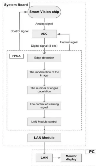
3. DESIGN OF THE SYSTEM 3.1 Structure of the surveillance system
The surveillance system as shown in Fig. 2 consists of a smart vision chip and the FPGA. The smart vision chip is composed of a general active pixel sensor(APS), a resistive network for smoothing the image, and a differential circuit designed by very large scale integration(VLSI) technology.
The analog output from the smart vision chip is converted into a digital signal through the analog digital converter(ADC), and then the digital output enters into the FPGA.
The FPGA acts the same as a central processing unit(CPU) in computers. The FPGA controls the smart vision chip, the ADC, and the Ethernet module to view the image and give a warning signal according to certain circumstances. It is also used for image processing. A hardware description language(HDL) was used to design the digital circuits for signal processing.
3.2 Detection of the number of edges
To generate a warning signal, we first count the number of edges for an object. The 8-bit ADC converts the output signal of the smart vision chip. The digital signal is separated from the edge signal or non-edge signal with a threshold algorithm by the FPGA. The range of the threshold that we set is a digital value between 124 and 130. If the digital value of a single pixel output converted from the ADC on the image is in the range of the threshold, this pixel has a non-edge signal. If the digital value of a single pixel output converted from the ADC for the image is out of the range of that threshold, this pixel has an edge signal from the object.(In this case, we define it as an ‘edge pixel’.) Fig. 3 shows a threshold algorithm. When the edge pixel is judged by the threshold algorithm, the digital value of a single pixel output converted from the ADC for the image is counted.
Fig. 1. Principle of edge detection. Fig. 2. Block diagram for the surveillance system.
4. MEASUREMENT 4.1 Measurement system
The designed surveillance system is composed of the smart vision chip, the bias circuits to adjust the image, an ADC, the FPGA, a light emitting diode(LED) for the warning signal, and a personal computer(PC) that already has designed software with Microsoft foundation library class(MFC) to confirm the image.
Fig. 4 shows a photograph of the system board. The FPGA functions as the microcontroller unit(MCU). It governs the control switches, the row decoder, the column decoder, and the reset decoder in the smart vision chip for the correct image. The ADC is also controlled by the FPGA with its datasheet. The Ethernet module can be connected to a PC to communicate via TCP/IP.
4.2 Measurement of light adaption with the smart vision chip
According to this vision chip principle[9], the only output is obtained by a differential intensity between the
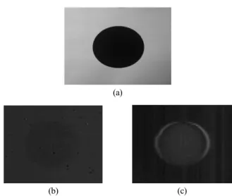
photoreceptors and the horizontal cells. Because of the use of a filtered image, the smart vision system sends a steady output image over a wide range of illumination conditions as compared with other image sensors[9]. During an actual measurement, the illumination range varied from 28 lux to 1150 lux, as shown in Fig. 5.
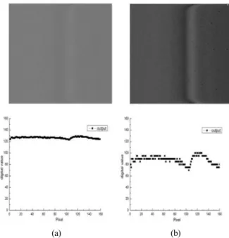
4.3 Modified edge signal for improved image
The range of the original analog output in the smart vision chip is only 350 mV, which is approximately a 27 in digital value[5]. Its output range is too small to clearly verify the object. The FPGA makes it possible to clarify the image by controlling the digital value, as shown in Fig. 6.
Fig. 7 shows experimental results of the difference between a non-modified image and a modified image. The graphs indicate the output of the 60throw below Fig. 7.
Fig. 3. Detection of the edge signal.
Fig. 5. Experimental results of the light-adaptive vision chip.
(a) original image, (b) 28 lux, (c) 1150 lux.
(a)
(b) (c)
(a) (b)
Fig. 6. Control of digital values.
(a) Original digital output of the smart vision chip, (b) Improved output digital signal.
Fig. 4. Photograph of the system board.
4.4 Remote surveillance system
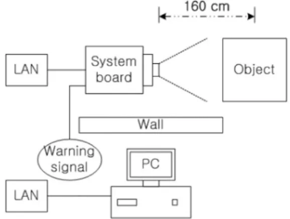
Since the Ethernet module has an original internet protocol(IP) address, when we input the IP address into our PC, the communication using TCP/IP makes it possible to view the remote images. Fig. 8 shows an experimental environment for the remote display. The PC is connected by a local area network(LAN) and the system board is distantly remote from the PC. Fig. 9 shows experimental results of the remote image with the environment.
As mentioned above, within the smart vision chip, the number of edges is counted by the FPGA. The object closest to the system has many edges, while the object furthest from the system board has relatively few edges within the image. We use this condition to provide the warning signal. Fig. 10 shows the number of the edges along with the distance from a circle with a 5 cm radius.
The threshold value for the warning signal is set as 1400.
LED is used to indicate a warning signal. Fig. 11 and Fig.
12 show the experimental environment for this study and the experimental results of the remote surveillance, respectively. In Fig. 12, we can confirm that the warning signal is turned-on if the object has a radius of > 10 cm, and the warning signal is turned-off if the object has a radius of < 5 cm, or is absent.
Fig. 8. Experimental environment for the remote display.
Fig. 9. Remote image with the environment.
Fig. 10. Number of the edges along with the distance for the circle of 5 cm radius.
Fig. 7. Experimental results of the improved image.
(a) Original output image, (b) Improved output image.
(a) (b)
5. CONCLUSION
In this paper, we proposed a remote surveillance system using a light-adaptive smart vision chip and a FPGA. The final output of the smart vision chip is the differential intensity between the output of the APS and the output of the resistive network. Because light intensity from the surroundings had less influence on the output, we could design the system for surveillance in low luminance. The FPGA was not only used to control the smart vision chip, the 8-bit ADC, the Ethernet module, and the warning signal, but was also used for image processing. For the remote surveillance system, we designed a printed circuit board(PCB) that can identify an image from a remote place using TCP/IP. Consequently, using the proposed threshold algorithm, the proposed system could be applied to a remote surveillance system.
ACKNOWLEDGMENT
This work was supported by a Korea Science and Engineering Foundation(KOSEF) grant funded by the Korea government(MEST) (No. 2010-0001878), the BK21 program and the Integrated Circuit Design Education Center(IDEC) in Korea.
REFERENCES
[1] H. Y. Hyun, J. S. Kong, and J. K. Shin, “Fundamental research of the target tracking system using a CMOS vision chip for edge detection”, J. Kor. Sensors Soc., vol. 18, no. 3, pp. 190-196, 2009.
[2] C. Y. Wu and C. F. Chiu, “A new structure of the 2-D silicon retina”, IEEE J. Solid-State Circuits, vol. 30, pp.
890-897, 1995.
[3] J.S. Kong, H.Y. Hyun, S.H. Seo, and J.K. Shin,
“Retina-motivated CMOS vision chip based on the column parallel architecture and switch-selective resistive network,” ETRI Journal, vol. 30, no. 2, pp.
783-789, December 2008.
[4] C. Y. Wu and C. F. Chiu, “A new structure of the 2-D silicon retina”, IEEE J. Solid-State Circuits, vol. 30, pp.
890-897, 1995.
[5] J.S. Kong, H.Y. Hyun, S.H. Seo, and J.K. Shin,
“Retina-motivated CMOS vision chip based on the column parallel architecture and switch-selective resistive network,” ETRI Journal, vol. 30, no. 2, pp.
783-789, December 2008.
[6] S.H. Suh, J.H. Kim, J.S. Kong, and J.K. Shin, “Vision chip for edge detection with a function of pixel FPN reduction”, J. Kor. Sensors Soc., vol. 14, no. 3, pp. 191- 197, 2005.
[7] J.S. Kong, S.H. Suh, S.H. Kim, J.K. Shin, and M.H.
Lee, “Resolution improvement of a CMOS vision chip for edge detection by separating photo-sensing and edge detection circuits”, J. Kor. Sensors Soc., vol. 15, no. 2, pp. 112-119, 2006.
[8] R. Takami, K. Shimonomura, S. Kameda, and T. Yagi,
“An image pre-processing system employing neuromorphic 100×100 pixel silicon retina[robot vision applications”, Circuits and Systems, ISCAS 2005.
IEEE International Symposium, vol. 3, pp. 2771 - 2774, 2005.
[9] S.K. Mendis, S.E. Kemeny, R.C. Gee, B. Pain, C.O.
Staller, Q. Kim, and E.R. Fossum, “CMOS active pixel
Fig. 11. Experimental environment for the remote surveillance.
Fig. 12. Experimental results of the remote surveillance system.
(a) No object,
(b) The object < 5 cm radius, (c) The object > 10 cm radius.
(a) (b) (c)
image sensors for highly integrated imaging systems”, IEEE Journal of Solid-State Circuits, vol. 32, pp. 187- 197, 1997.
[10] J.H. Kim, J.H. Park, J.K. Shin, and M.H. Lee,
“Analysis of local light adaptation mechanism in a biologically motivated CMOS vision chip for edge detection”, IEEE Int. Conf. Neural Networks and Signal Processing, vol. 1, pp. 275-278, 2003.
[11] H. Okuno and T. Yagi, “Real-time robot vision for collision avoidance inspired by neuronal circuits of insects”, Proc. of the 2007 IEEE/RSJ Int. Conf. on Intelligent robots and systems, pp. 1302-1307, 2007.
[12] H. Yamada, T. Miyashita, M. Ohtani, K. Nishio, H.
Yonezu and Y. Furukawa, “An integrated circuit for two-dimensional edge-detection with local adaptation based on retinal networks”, Optical Review, vol. 9, no.
1, pp. 1-8, 2002.
[13] R. Takami, K. Shimonomura, S. Kameda and T. Yagi,
“An image pre-processing system employing neuromorphic 100×100 pixel silicon retina”, Proc.
IEEE Intl. Symp. On Circuits and Systems, 2005.
[14] H. Okuno and T. Yagi, “Bio-inspired real-time robot vision for collision avoidance”, Journal of Robotics and Mechatronics, vol. 20, no.1, 2008.
[15] J.S. Kong, S.H. Jo, S. Lee, K.H. Choi, S.H. Seo and J.K. Shin, “Operation of a wide dynamic range CMOS image sensor based on dual sampling mechanism and its SPICE simulation”, J. Kor. Sensors Soc., vol. 19, no. 4, pp. 285-290, 2010.
[16] S. Lee, S.H. Seo, J.S. Kong, S.H. Jo, K.H. Choi, P.
Choi and J.K. Shin, “Dynamic range extension of the n-well/gate-tied PMOSFET-type photodetector with a built-in transfer gate”, J. Kor. Sensors Soc., vol. 19, no. 4, pp. 328-335, 2010.
Kyung-Hwa Choi received the BE degree in electrical engineering and computer science from Kyungpook National University, Daegu, Korea, in 2008, and ME degree in sensor and display engineering from the same university. His current fields of interest are in the CMOS vision chip and its applications.
Sung-Hyun Jo received the BE and ME degree in electrical engineering and computer science from Kyungpook National University, Daegu, Korea, in 2008 and 2011, respectively. He is now working for the PhD degree at the same university. His current fields of interest are in the CMOS image sensor and its applications.
Sang-Ho Seo received his BE degree in electronic engineering from Kyungpook National University, Daegu, Korea, in 2002 and ME degree in electronics from the same university in 2004. In 2009, he received the PhD degree from the same university. Now he is working for Samsung Mobile Display.
Jang-Kyoo Shin received his BE degree in electronic engineering from seoul national university, Seoul, Korea, in 1978 and MS degree in electrical engineering from Korea Advanced Institute of Science and Technology, Korea, in 1980. He received the PhD degree in electrical engineering from colorado State University, Fort Collins, USA in 1991. He is now a Professor in the School of Electronics Engineering at Kyungpook National University, Daegu, Korea. His current fields of interest are semiconductor sensors and intelligent sensor systems.