http://dx.doi.org/10.5369/JSST.2011.20.5.289 pISSN 1225-5475/eISSN 2093-7563
Synthesis and Sensing Properties of Pd Nanoparticle- Functionalized SnO
2Nanowires
Katoch Akash, Sun-Woo Choi, Eun-Kyeong Kim, and Sang Sub Kim+
Abstract
Networked SnO2nanowires were uniformly functionalized with Pd nanoparticles via γ-ray radiolysis. The Networked SnO2nanowires were fabricated through a selective growth method. The sensing properties of the Pd-functionalized SnO2nanowires were analyzed in terms of their response to NO2and CO gases. The response time and sensitivity of the sensors were significantly improved for NO2at lower temperatures by the Pd functionalization. The enhancement in the sensing properties is likely to be due to the spillover effect of the Pd nanoparticles.
Keywords : Gas Sensor, Nanowire, Pd-SnO2, Functionalization
1. INTRODUCTION
Oxide nanostructures have been widely studied for their potential use in chemical gas sensors. Specially, one- dimensional oxide nanowires have received much attention, in comparison to traditional sensors based on thin or thick films of nanoparticles, due to their peculiar physical and chemical properties. One-dimensional oxide nanostructures based on nanowires, nanotubes and nanoribbons exhibit excellent sensitivity for gas detection due to their exceptionally high surface-to-volume ratio, single crystalline nature, and semiconducting electrical behavior[1-3].
However, sensors based on single nanowire have some shortcomings which restrict their practical applications[4].
First, their fabrication requires a careful photolithography process, usually involving tedious fabrication steps.
Second, an expensive measurement unit is required for gauging the infinitesimal current change due to the interaction of gaseous species with the surface of the nanowires. Third, the different sizes of each nanowire used for sensing may alter the current values. In comparison to single nanowire sensors, networked nanowires are superior in terms of fabrication and reproducibility, but suffer with lower sensitivity and longer response times. These properties need to be improved in order to see them applied
practically.
Meanwhile, metallic nanoparticles can be used as a catalyst to enhance the properties of gas sensors[5]. These metallic catalysts facilitate a spillover effect, which involves a dissociation of gaseous species into ions or neutral chemical species, resulting in superior gas sensing capability[6]. Various methods have been attempted to functionalize oxide nanowires with metallic catalysts[7-9].
Radiolysis is one effective route for synthesizing metallic nanoparticles and can also be employed to functionalize nanowires[10-12].
In this work, we fabricate networked SnO2nanowires via a selective growth method. Subsequently, the nanowires are Pd-functionalized through γ-ray radiolysis. We investigate the sensing properties of the Pd-functionalized SnO2nanowires at different temperatures in terms of their response to NO2and CO.
2. EXPERIMENTAL DETAILS
The fabrication of Pd-functionalized SnO2networked nanowire sensors involves two steps. First, the SnO2 nanowires were selectively grown on patterned interdigital electrodes(PIEs) by the well-known vapor-liquid-solid growth method. Second, the Pd nanoparticles were functionalized on the surface of the SnO2nanowires by γ- ray radiolysis. The PIEs were prepared on SiO2/Si(100) substrates using a conventional lithography process followed by the deposition by sputtering of tri-layers
School of Materials Science and Engineering, Inha University, Incheon 402-751, Republic of Korea
+Corresponding author: [email protected]
(Received : Jul. 20. 2011, Revised : Sep. 10. 2011, Accepted : Sep. 15. 2011)
composed of Au(3 nm)/Pt (100 nm)/Ti (100 nm). The Ti (100 nm) layer was deposited to provide better adhesion between the Pt and SiO2layers. The SnO2nanowires with network junctions were selectively grown on 10-nm-spaced PIEs. The conditions used for fabrication of the SnO2 nanowires are described in detail in our previous report[13].
The precursor solution for the functionalization of the SnO2nanowires with Pd nanoparticles was prepared by dissolving 0.051 mM of palladium chloride(PdCl2, Kojima Chemicals Co.) in a mixed solvent of acetone(50 vol%) and 2-propanol(50 vol%). The prepared solution was stirred for 24 h. Then the fabricated networked SnO2 nanowires were immersed in the precursor solution. The solution was illuminated with 60Co γ-rays for 3 h in ambient air at room temperature at the Korea Atomic Energy Research Institute(KAERI). The prepared samples were heat treated at 500 。C for 1 h in air.
The microstructure of the Pd-functionalized SnO2 nanowires was investigated using field-emission scanning electron microscopy(FE-SEM) and transmission electron microscopy(TEM). Their responses to NO2and CO were measured using a custom-made sensing system. The measurements were taken at various temperatures. The response(R) was estimated as R = Rg/Ra, where Rais the resistance in the absence of NO2and Rgis the resistance measured in the presence of NO2. The converse was applied for the case of CO.
3. RESULTS AND DISCUSSIONS
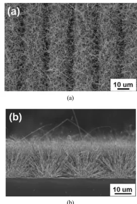
Fig. 1a and 1b show the plan- and the cross-section views of the networked SnO2 nanowires, which demonstrate the formation of networked junctions on the PIEs by the selective growth method. The Pd nanoparticles were anchored to these nanowires by γ-ray radiolysis. Fig.
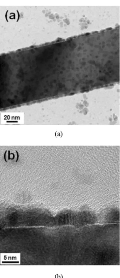
2a and 2b show low and high magnification images of the Pd-functionalized networked SnO2 nanowires. Fig. 2b clearly shows that the Pd nanoparticles were uniformly deposited on the surface of SnO2nanowires. The average diameter of the Pd nanoparticles is ~20 nm. The microstructure of the Pd nanoparticles on the surface of SnO2nanowires was further investigated by TEM. The results are shown in Fig. 3. Fig. 3a clearly reveals a uniform dispersion of the Pd nanoparticles on the surface of an SnO2nanowire. The high resolution TEM image in Fig. 3b displays the lattice fringes of an SnO2nanowire and Pd nanoparticles. The lattice spacing confirms the
successful formation of single-crystalline SnO2nanowires and Pd nanoparticles.
(a)
(b)
Fig. 1. (a) Plan view of the networked SnO2nanowires grown on patterned electrodes via the selective growth method. (b) Cross-sectional view of the networked SnO2nanowires.
(a)
(b)
Fig. 2. (a) Plan view of the networked SnO2nanowires functionalized with Pd nanoparticles through γ-ray radiolysis. (b) Microstructure of the Pd nanoparticles on the surface of the SnO2nanowires grown under 10 kG h-1 60C γ-rays for 3 h.
The sensing properties of the Pd-functionalized networked SnO2nanowires were tested in temperatures from 50 to 300 。C for NO2. The obtained results are shown in Fig 4. The resistance of the Pd-functionalized SnO2nanowires tracked the supply/cut off of NO2 well.
The response time decreases from 140 to 20 s as the temperature is raised from 50 。C to 200 。C. Whereas at 300 。C, the response time has risen back to 100 s. The best sensing properties were obtained at 200 。C, as shown in Fig. 4d. The inset of the figure shows an enlarged part of the result obtained at 0.1 ppm NO2 for clarity. This variation in resistance of the Pd-functionalized networked SnO2 sensors can be explained by the n-type semiconductor mechanism and the spillover effect of the Pd nanoparticles.
In bare SnO2nanowires, the resistance increases upon exposure to NO2and decreases upon removal of NO2. The NO2molecules adsorbed on the surface of SnO2nanowires are likely to extract electrons from the surface region of SnO2 nanowires, enhancing the surface depletion of each SnO2 nanowire. The extracted electrons are then transferred back to the conduction band of the SnO2
nanowires in conjunction with the desorption of the NO2 molecules.
The Pd nanoparticles on the surface of the SnO2 nanowires provide more active sites for adsorption of NO2 molecules through the spillover effect[6]. The spillover effect facilitates the adsorption of NO2molecules. More adsorption of NO2 molecules is likely to enhance the depletion region and suppress the underlying conducting channel more. The overall effect reduces the conductance, which ultimately lowers the response time and enhances the sensitivity. Another possibility is that the Pd nanoparticles induce catalytic effects and dissociate the NO2into ions or neutral chemical species, such as NO, O, NO2-, NO+and NO-[14-17]. These chemical species tend to capture the electrons in SnO2nanowires, enhancing the sensing properties.
The sensitivity of the Pd-functionalized SnO2nanowires at different temperatures is shown in Fig. 4f. They show an exceptionally high response at 200 。C. As the temperature is raised, the response also increases gradually. This is likely to be due to the faster adsorption and desorption of chemical species at higher temperatures.
The sensing behavior of the Pd-functionalized SnO2 nanowires was also investigated in the presence of CO at
(a)
(b)
Fig. 3. TEM images of the Pd nanoparticles on the surface of the SnO2nanowires at (a) low and (b) high magnification.
Fig. 4. Response curves of the Pd-functionalized SnO2nanowire sensor to NO2at (a) 50 。C, (b) 100 。C, (c) 150 。C, (d) 200 。C and (e) 300 。C. (f) Summary of responses obtained from the Pd- functionalized SnO2nanowires.
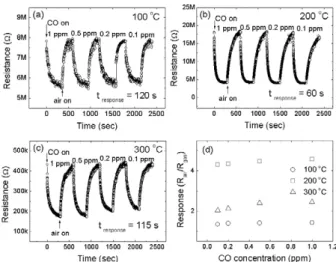
temperatures from 100 。C to 300 。C. A typical response curve we obtained is shown in Fig. 5. The sensor shows a relatively long response time and a low response to CO.
The best response time of 60 s was obtained at 200 。C.
The response is summarized in Fig. 5d. According to the results, it is reasonable to conclude that the Pd- functionalized SnO2nanowires are more sensitive to NO2 than to CO.
4. CONCLUSIONS
Pd nanoparticles were successfully functionalized on the surface of the networked SnO2nanowires via γ-ray radiolysis. The Pd-functionalized SnO2nanowires showed reasonable response times and responses to NO2at 200 。C.
On the other hand, the sensor was not sensitive to CO.
ACKNOWLEDGMENT
This work was supported by Nuclear R&D program through the National Research Foundation of Korea.
REFERENCES
[1] M. Law, H. Kind. B Messer, F. Kim, and P. Yang,
“Photochemical sensing of NO2with SnO2nanoribbon nanosensors at room temperature”, Angew. Chem. Int.
Ed., vol. 41, pp. 2405-2408, 2002.
[2] B. Wang, L. F. Zhu, Y. H. Yang, N. S. Xu, and G. W.
Yang, “Fabrication of SnO2 nanowire gas sensor and sensor performance for hydrogen”, J. Phys. Chem. C, vol. 112, pp. 6643-6647, 2008.
[3] W.-S. Kim, B.-S. Lee, D.-H. Kim, H.-C. Kim, W.-R.
Yu, and S.-H. Hong, “SnO2nanotubes fabricated using electrospinning and atomic layer deposition and their gas sensing performance”, Nanotechnology, vol. 21, p.
245605, 2010.
[4] J. Y. Park, D. E. Song, and S. S. Kim, “An approach to fabricating chemical sensors based on ZnO nanorod arrays”, Nanotechnology, vol. 19, p. 105503, 2008.
[5] C. D. Zorzi, G. Rossetto, D. Calestani, M. Z. Zha, A.
Zappettini, L. Lazzarini, M. Villani, N. E. Habra, and L.
Zanotti, “Pd/PdO functionalization of SnO2nanowires and ZnO nanotetrapods”, Cryst. Res. Technol., vol. 46, pp. 847-851, 2011.
[6] C. Wang, L. Yin, L. Zhang, D. Xiang, and R. Gao,
“Metal oxide gas sensors: sensitivity and influencing factors”, Sensors, vol. 10, pp. 2088-2106, 2010.
[7] P. Paiano, P. Prete, E. Speiser, N. Lovergine, W.
Richter, L. Tapfer, and A. M. Mancini, “GaAs nanowires grown by Au-catalyst-assisted MOVPE using tertiarybutylarsine as group-V precursor”, J.
Cryst. Growth, vol. 298, pp. 620-624, 2007.
[8] T. Aichele, A. Tribu, G. Sallen, J. Bocquel, E. B.
Amalric, C. Bougerol, J. P. Poizat, K. Kheng, R. Andre, S. Tatarenko, and H. Mariette, “CdSe quantum dots in ZnSe nanowires as efficient source for single photons up to 220 K”, J. Cryst. Growth, vol. 311, pp. 2123- 2127, 2009.
[9] S. S. Kim, J. Y. Park, S.-W. Choi, H. S. Kim, H. G. Na, J. C. Yang, C. Lee, and H. W. Kim, “Room temperature sensing properties of networked GaN nanowire sensors to hydrogen enhanced by the Ga2Pd5 nanodot functionalization”, Int. J. Hydrogen Energy, vol. 36, pp. 2313-2329, 2011.
[10] S. P. Ramnani, J. Biswal, and S. Sabharwal,
“Synthesis of silver nanoparticles supported on silica aerogel using gamma radiolysis”, Radiat. Phys.
Chem., vol. 76, pp. 1290-1294, 2007.
[11] T. Li, H. G. Park, and S.-H. Choi, “γ-Irradiation- induced preparation of Ag and Au nanoparticles and their characterizations”, Mater. Chem. Phys. vol. 105, pp. 325-330, 2007.
[12] S. Chettibi, Y. Benguedouar, and N. Keghouche, “The metal-support interaction in the oxide supported nickel
Fig. 5. Response curve of the Pd-functionalized SnO2nanowire sensor to CO at (a) 100 。C, (b) 200 。C, and (c) 300 。C. (d) Summary of responses obtained from the Pd-functionalized SnO2nanowires.
nanoparticles synthesized by radiolysis”, Phys.
Procedia, vol. 2, pp. 707-712, 2009.
[13] S.-W. Choi, S.-H. Jung, and S. S. Kim, “Functionali- zation of selectively grown networked SnO2nanowires with Pd nanodots by γ-ray radiolysis”, Nanotechno- logy, vol. 22, pp. 225501, 2011.
[14] J. Tamaki, M. Nagaishi, Y. Teraoka, N. Miura, N.
Yamazoe, K. Moriya, and Y. Nakamura, “Adsorption behavior of carbon monoxide and interfering gases on tin dioxide”, Surf. Sci., vol. 221, pp. 183-196, 1989.
[15] B. Ruhland, T. Becker, and G. Muller, “Gas-kinetic
interactions of nitrous oxides with SnO2surfaces”, Sens. Actuators B, vol. 50, pp. 85-94, 1998.
[16] J.-H. Park, D.-G. Lim, Y.-J. Choi, D.-W. Kim, K.-J.
Choi, and J.-G. Park, “Laterally grown SnO2 nanowires and their NO2gas sensing characteristics”, Int. Conf. on Nanotechnology, pp. 1054-1057, Hong Kong, 2007.
[17] J. Y. Park, S.-W. Choi, and S. S. Kim, “Junction-tuned SnO2nanowires and their sensing properties”, J. Phys.
Chem. C, vol. 115, pp. 12774-12781, 2011.
Katoch Akash received a BS from Himachal Pradesh University, India, in 2004. In 2009, he received his MS degree from Thapar University, He is currently a doctoral course student at Inha University. His research topic is oxide nanowires/nanofibers gas sensors.
Eun-Kyeong Kim received a BS degree from Inha University, Republic of Korea in 2010. She is currently a master course student at Inha University.
Her research topic is hydrophilic/phobic thin films.
Sun-Woo Choi received his BS and master degrees from Inha University, Republic of Korea, in 2008 and 2010, respectively.. He has been a doctoral student at Inha University from 2010.
He is working on metal oxide gas sensors and synthesis of metal nanoparticles.
Sang Sub Kim received his PhD from Pohang University of Science and Technology in 1994 on the topic of material science and engineering. He is a Professor of Materials Science and Engineering at Inha University. His research interests include the synthesis and characterization of nanomaterials.