A 2.7Gbps & 1.62Gbps Dual-Mode Clock and Data Recovery for DisplayPort in 0.18µm CMOS
Seung-Won Lee*, Tae-Ho Kim**, Suk-Won Lee*, Jin-Ku Kang**★
Abstract
This paper describes a clock and data recovery (CDR) circuit that supports dual data rates of 2.7Gbps and 1.62Gbps for DisplayPort standard. The proposed CDR has a dual mode voltage-controlled oscillator (VCO) that changes the operating frequency with a “Mode” switch control. The chip has been implemented using 0.18µm CMOS process. Measured results show the circuit exhibits peak-to-peak jitters of 37ps(@2.7Gbps) and 27ps(@1.62Gbps) in the recovered data. The power dissipation is 80㎽ at 2.7Gbps rate from a 1.8V supply.
Key words: clock and data recovery(CDR), voltage-controlled oscillator(VCO), DisplayPort, half-rate PD
* Samsung Electronics co.
** School of Electronics Engineering, Inha University
★Corresponding author
※ Acknowledgment
This work is supported by Human Resource Training Project for Strategic Technology from KIAT, and IDEC program.
Manuscript received Mar. 4, 2010 ; revised Mar. 25, 2010
I. Introduction
CDR circuits are used extensively in high-speed digital interface systems such as Ethernet receivers, disk drive read and write channels, digital mobile receivers, and high-speed interfaces to extract timing information from data. DisplayPort is a high-speed digital display serial interface standard set by the Video Electronics Standards Association (VESA) for high-resolution display devices. The DisplayPort source transmits data only in serial and the sink device should recover clock from the input data. Therefore the CDR circuit is the most important block in the front end of the receiver side. Main Link of DisplayPort operates at dual link rates: 2.7Gbps and 1.62Gbps per lane[1]. So, the CDR for the DisplayPort sink device should work at
two different data rates.
In this paper, we present a CDR which handles dual data rates, 2.7Gbps and 1.62Gbps for DisplayPort. The CDR with a dual mode VCO frequency by single mode switching control is proposed.
Section II gives the CDR architecture and operating principle. Details of the building block are given in section III. The measurement results are given in section IV.
II. Architecture
Fig. 1. Proposed CDR Architecture
The proposed CDR employs a dual-loop
architecture CDR[2]. The structure of a dual-loop CDR based on external reference (using the external reference is optional according to DisplayPort standard) is shown in Fig. 1. The dual-loop topology includes a phase-locked loop and a frequency-acquisition loop. The frequency- acquisition loop consists of a phase frequency detector (PFD), a charge pump (CP), a multiplexer (MUX), a loop filter, dividers, and 4-stage ring oscillator. The phase- locked loop includes a half-rate linear phase detector (PD), a CP, and shares a MUX, a loop filter, and a VCO with the frequency-acquisition loop. During startup process, a phase frequency detector (PFD) compares the frequency difference between an external reference clock and recovered clock. When the frequency difference is less than about 1000ppm, a lock detector sends the lock signal and sets the MUX to switch from the frequency-acquisition loop to the phase-locked loop.
The phase-locked loop also can be changed with frequency detector instead of frequency-acquisition loop without an external reference clock.
At the same time, the serial input data is provided to a half-rate linear phase detector (PD) and the lock detector turns the PFD off during phase-locked loop operation in order to prevent the up/down pulses of the PFD from interfering with the loop filter through the MUX. The phase-locked loop recovers clock and data from received the random input signals. The half-rate clocks are used for data recovery, and thus the recovered data are in a 2-bit de-serialized format. The 2-bit recovered data are multiplexed by a selector for measurement. The selector block can be omitted or modified depending on the following digital block. Current Mode Logic (CML) gates are designed for proper operation at giga-bit range in PD, selector and output buffers.
The DisplayPort should support serial 2.7Gbps and 1.62Gbps data, respectively. A “mode” selecting signal is used for changing the divider ratio and tuning the center frequency of the VCO. Since the ratio of 2.7Gbps and 1.62Gbps is 5 : 3, the divider ratio is selected between divide-by-5 divider and divide-by-3 divider by the mode signal. The VCO should generate the 1.35㎓ clock and 810㎒ clock since the CDR is the half-rate architecture.
The CDR utilizes the “Link Training” period for the CDR lock in DisplayPort Standard[1]. The lock information is sent to the DPCD (DisplayPort Configuration Data) through AUX (Auxiliary) channel. In this process, the DisplayPort source device sends the D10.2 pattern to the CDR. This pattern is used for the reference-less CDR architecture. Since the proposed CDR uses the external reference, it can still be locked at D10.2(0101.. pattern) pattern. In the “Link Training”
process, a value of address 100h in the DPCD can be used for the “Mode” signal.
Ⅲ Building Block 1. VCO
The VCO generates clock signals for the half-rate linear PD. Since the CDR should support two different data rates, the VCO also should generate outputs that have different frequencies. Using two narrow frequency ranges has smaller gain than
(a)
(b)
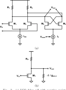
Fig. 2. (a) VCO delay cell with negative-resistance load (b) half-circuit
wide frequency range prototypes.
It results a small loop filter, chip area and low jitter performance. In this paper, we propose a ring oscillator that can change the operating frequency by single mode switching control.
Fig. 2(a) shows the widely used delay cell of VCO using positive feedback[3]. Fig. 2(b) shows the half circuit equivalent of Fig. 2(a). The load of the differential pair consists of resistors R1 and R2 (R = R2 = RP) and the cross-coupled pair M3-M4. As IC
increases, the small-signal differential resistance -2/gm3,4 becomes less negative. And from the half circuit of Fig. 2(b), the equivalent resistance increases as given in Eq. (1).
·
(1) Thus the frequency of oscillation is determined by Eq. (2).
∝·
(2)
Fig. 3(a) shows the proposed delay cell of VCO.
Two additional current sources are added to the conventional delay cell for Mode switching. By adding two current sources (I1, I2) to the differential amplifier stage and negative Gm stage respectively, the VCO gain curve exhibits two different mode operations.
By the proposed scheme, the VCO center frequency can be controlled while the VCO gain remains almost constant. The suitable current values for the VCO gain to remain the same can be determined. As described earlier, the VCO frequency change can be done by single switching control. In the beginning, the “Mode” switch is off. Thus the VCO is operating at 810㎒ and the CDR selects the divide-by-5 divider. If the “Mode” switch is turned on, the CDR selects the divide-by-3 divider. At the same time, the current source I2 is turned on and I1
is turned off, then the VCO operates at 1.35㎓.
The frequency switching operation is described in detail as below.
(a)
A (Mode on)
B (Mode off)
Control voltage (V)
(b)
Fig. 3. (a) Proposed VCO delay cell (b) VCO characteristics with ‘Mode’ switch
1) In the case of adding I1 : According to (1) and (2), adding I1 makes the VCO frequency lower due to the increase of equivalent resistance. Assuming that Vcont changes from 0 to VDD, the frequency variation by Vcont is smaller than the former case since the current variation by Vcont is relatively small in comparison with I1. So, the center frequency of the VCO and the VCO gain decrease.
The line ‘B’ in Fig. 3(b) shows the VCO gain curve when I1 is added.
2) In the case of adding I2 : According to (1) and (2), adding I2 does not affect Req, so the frequency of the VCO remains the same when Vcont
is 0. But the DC value of the Vout node decreases since IRp drop increases. Also, the source voltage of M3 and M4 (the drain of current source IC) decreases. Therefore, the current produced by Vcont
is smaller, thus the VCO gain decreases. The line
‘A’ in Fig. 3(b) shows the VCO gain curve when I2
is added.
As shown in Fig. 3(b), for two different modes the VCO gain stays almost the same at about 800- 900㎒/V.
2. Phase Detector
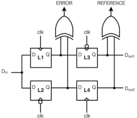
The Fig. 4 shows the half-rate linear phase detector[4]. It consists of four latches and two XOR gates. The data is applied to two sets of cascaded latches, each cascade constitutes a flip-flop. In this work, latches and XORs are implemented with CML logic. Since the flip-flops are driven by a half-rate clock, they de-multiplex the original input sequence if the clock samples the data in the middle of the bit eye. The basic unit employed in the circuit is a latch whose output tracks its input for the half of the clock period and holds its value for the other half. The error signal is equal to ONE only if a data transition has occurred. Since the input data is random in nature and the clock is periodic the average value of the error signal is pattern dependent. To convey this dependence, a reference signal is generated. The width of the error pulses is only half of the reference pulses in the lock condition. This dictates the scaling the amplitude of the error signal up by a factor of two. The difference between their average values in the lock condition drops to zero and the phase error continues to be linearly proportional to the difference in the vicinity of lock.
Fig. 4. Half-rate linear phase detector
3. Charge Pump
The charge pump is shown in Fig. 5. A unity-gain buffer is used to clamp the terminal voltages of current sources during the zero-current pumping period. In this way, voltage glitches on the loop filter due to charge sharing can be eliminated.
Both the up and the down current can be either connected to the output or drained to a dummy reference voltage by the four switches. To minimize clock feedthrough, all switches are implemented by an NMOS and a PMOS transistor, and every transistor has its own control signal, and the relative timing is optimized to avoid glitches in the output.
The UP and DN current of charge pump in phase-locked loop is 10µA and 20µA since the circuit uses the half-rate linear phase detector. The current of charge pump in frequency-acquisition loop is 100µA.
Fig. 5. Charge pump 4. Frequency lock Detector
The frequency lock detector block is given in Fig.
6. If the VCO clock edge stays within a fixed delay range over than the setting time period, the lock signal is generated. The delay is used from VCO delay cell and 5 bit counter is implemented. If more
Fig. 6. Frequency lock detector
precise lock control is needed, the counter size could be increased.
Ⅳ Measurement Results
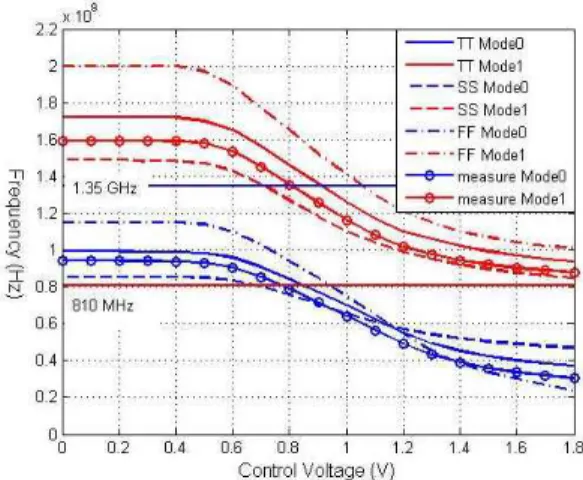
The chip has been implemented using 0.18µm CMOS process. Fig. 7 shows the chip photo. The capacitances of 5.3pF and 500fF were used for loop filter and were implemented using MOS capacitance for saving chip area. Fig. 8 shows simulated VCO tuning range under the hardest corner conditions of SS(slow-slow), TT(typical-typical) and FF(fast- fast) with temperature, supply voltage after layout parasitic extraction and measurement result after fabrication.
Upper four curves are in 2.7Gbps mode and the center frequency of those is 1.35㎓. Lower four curves are in 1.62Gbps mode and the center frequency of those is 810㎒. The gain of VCO is about 900㎒/V within the valid control voltage range(0.6V∼1.3V) for two different data rates.
Fig. 7 Chip photo
(FLD: Frequency Lock Detector, CP: Charge Pump, LF: Loop Filter VCO: Voltage Controlled Oscillator,
OD: Output Driver)
Fig. 8. VCO tuning range post simulation &
measurement (upper: 1.35㎓, lower: 810㎒)
Lock time is about 400ns in simulation when the
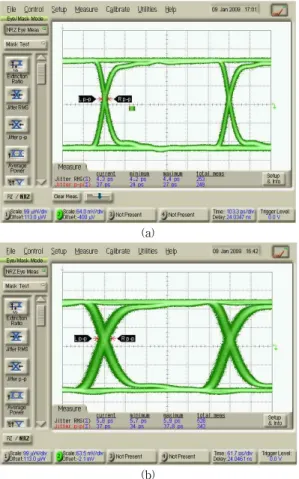
“Mode” signal is changed. This result is within the DisplayPort electrical specification, in which the CDR should be locked within 100µs[1]. Since the lock detector was implemented with a delay circuit and a counter for measuring the frequency sustaining, the delay value and bit size of the counter can be adjusted on the lock time performance. If the counter bit size is increased, more precise lock detection can be implemented. In this circuit we used about 1000ps delay circuit and 5 bit counter. Fig. 9 shows the measured eye diagrams of 2.7Gbps and 1.62Gbps recovered data.
The 2.7Gbps output data-eye exhibits a pick-to-pick jitter of 37ps and the 1.62Gbps output data-eye exhibits a pick-to-pick jitter of 27ps, respectively.
Fig. 10 illustrates the jitter tolerance at 2.7Gbps. It shows the circuit meets the jitter tolerance specification of the DisplayPort. The loop bandwidth is set as 20㎒ as specified in the standard.
Our work was compared to recently published work[5], which is designed for the same target as the DisplayPort standard. Our work shows a better jitter performance with a little more power consumption. The lower jitter comes from a little more current for Mode switching in the VCO cell.
The performance comparison of the proposed CDR is given in Table 1.
(a)
(b)
Fig. 9. (a) 1.62Gbps output data-eye (pk-pk jitter:27ps) (b) 2.7 Gbps output data-eye (pk-pk jitter:37ps)
Fig. 10. Jitter tolerance
Table 1. Performance Comparison
[5] This work
process CMOS 0.18µm
1P-6M CMOS 0.18µm 1P-6M
Supply voltage 1.8V 1.8V
Data rate 2.7Gbps &
1.62Gbps 2.7Gbps &
1.62Gbps
Bandwidth 20㎒ 20㎒
Peak-to-peak
jitter [email protected]
[email protected] [email protected] [email protected] power
consumption 50㎽ @2.7Gbps 80㎽ @2.7Gbps
Ⅴ Conclusion
A CDR circuit that supports dual data rates of 2.7Gbps and 1.62Gbps for DisplayPort sink device is presented in this paper. With the proposed VCO circuit, the data rate of CDR can be selected by single mode switching control. The CDR circuit is designed in a 0.18µm CMOS technology. Measured results show the circuit exhibits peak-to-peak jitters of 37ps(@2.7Gbps) and 27ps(@1.62Gbps) in the recovered data. The power dissipation is 80㎽ at 2.7Gbps rate from a 1.8V supply.
References
[1] VESA, DisplayPort Standard, Version 1, Revision 1a, January 2007.
[2] L. Henrickson, et al., "Low-Power Fully Integrated 10-Gb/s SONET/SDH Transceiver in 0.13-µm CMOS," IEEE Journal of Solid-State Circuits, vol.38, no.10, pp.1595-1601, October 2003.
[3] B. Razavi, Design of Analog CMOS Integrated Circuits, New York, McGraw-Hill, pp.482-531, 2001.
[4] J. Savoj, B. Razavi, "A 10-Gb/s CMOS Clock and Data Recovery Circuit with a half-Rate Binary Phase/Frequency Detector," IEEE Journal of Solid-State Circuits, vol.38, no.1, pp. 13-21, January 2003.
[5] Chorng-Sii Hwang, et al., "Dual-Band CDR using a Half-Rate Linear Phase Detector," IEEE International of SOC Conference, pp.51-54, September 2009.
Tae-Ho Kim (Student Member) 2007 : BS degree in Electronics Engineering, Inha University.
2009 : MS degree in Electronics Engineering, Inha University.
2009 ~ : PhD candidate in Electronics Engineering, Inha University.
Suk-Won Lee (Member)
2008 : BS degree in Electronics Engineering, Inha University.
2010 : MS degree in Electronics Engineering, Inha University.
2010 ~ Present : Research Engineer, Samsung Elecronics.
Jin-Ku Kang (Member)
1983 : BS degree in Nuclear Engineering, Seoul National University.
1990 : MS degree in Electrical and Computer Engineering, New Jersey Institute of technology.
1996 : PhD degree in Electrical and Computer Engineering, north Carolina State
University.1983~1988 : Research Engineer, Samsung Electronics.
1996~1997 : Senior Design Engineer, Intel(U.S).
1997 ~ Present : Professor, Inha University BIOGRAPHY
Seung-Won Lee (Member)
2007 : BS degree in Electronics Engineering, Inha University.
2009 : MS degree in Electronics Engineering, Inha University.
2009 ~ Present : Research Engineer, Samsung Electronics.