Al 그리드와 ZnO 투명전도막 의 공정변화에 따른 Cu(In,Ga)Se
2박막태양전지의 특성 연구
조보환ㆍ김선철ㆍ문선홍ㆍ김승태ㆍ안병태*
한국과학기술원 신소재공학과, 대전시 유성구 대학로 291, 305-338
Effect of Process Variation of Al Grid and ZnO Transparent Electrode on the Performance of Cu(In,Ga)Se
2Solar Cells
Bo Hwan Cho ․ Seon Cheol Kim ․ Sun Hong Mun ․ Seung Tae Kim ․ Byung Tae Ahn*
Department of Materials Science and Engineering, KAIST, Daehak-ro 291, Yuseong-goo, Daejeon 305-338, Korea
ABSTRACT: CIGS solar cell consisted of various films. In this research, we investigated electrode materials in Cu(In,Ga)Se2(CIGS) cells, including Al-doped ZnO (ZnO:Al), intrinsic ZnO (i-ZnO), and Al films. The sputtered ZnO:Al film with a sputtering power at 200W showed the lowest series resistance and highest cell efficiency. The electrical resistivity of the 200-W sputtered ZnO:Al film was 5.2x10⁻⁴ Ω·cm by the rapid thermal annealing at 200°C for 1 min. The electrical resistivity of i-ZnO was not measurable due to its high resistance. But the optical transmittance was highest with less oxygen supply and high efficiency cell was achieved with O2/(Ar+O2) ratio was 1% due to the increase of short-circuit current. No significant change in the cell performance by inserting a Ni layer between Al and ZnO:Al films was observed.
Key words: CIGS solar cell, ZnO:Al, i-ZnO, elect rode(Al/Ni) film
*Corresponding author: [email protected]
Received February 15, 2015; Revised February 16, 2015;
Accepted February 23, 2015
ⓒ 2015 by Korea Photovoltaic Society
This is an Open Access article distributed under the terms of the Creative Commons Attribution Non-Commercial License (http://creativecommons.org/licenses/by-nc/3.0)
which permits unrestricted non-commercial use, distribution, and reproduction in any medium, provided the original work is properly cited.
Nomenclature
CIGS : Cu(In,Ga)Se2
ZnO:Al : Al-doped zinc oxide film i-ZnO : intrinsic zinc oxide film Voc : open-circuit voltage, V Jsc : short-circuit current, mA/cm2 FF : fill factor
Subscript
XRD : x-ray diffraction
SEM : scanning electron micorscopy QE : quantum efficiency
1. 서 론
태양전지는 다양한 층 들이 증착 되어서 하나의 Cell로 구성 되는 구조이다. 그 구조에는 Mo, CIGS absorber, CdS, i-ZnO, ZnO:Al, electrode film들이 포함되어 있다1). 본 실험에서는 구 조 중 위쪽에 해당되는 층들을 세가지 의 Part로 나누어서 진행 할 것이다.
첫 번째는 ZnO:Al 층이다. ZnO:Al 층은 high electric con- ductivity, high temperature-stability, low cost, non-toxicity의 이점을 가지고 있다2-4). 이러한 장점은 thin film Solar cell에서 front contact 층으로 사용되고 있다5-6). i-ZnO 층 뿐만 아니라 고 효율 Cell 제작에 영향을 미친다. 좋은 특성을 가지는 ZnO:Al을 얻기 위해서는 Power, 두께, Working pressure, substrate tem- perature 등의 조건들을 변화 시키게 된다. 이번 실험에서는 ZnO:Al을 제작 시 Power의 변화를 주어 생성된 film의 변화와 이를 Cell에 적용하게 되었을 때의 Photovoltaic properties에 대 해서 알아 볼 것이다.
두 번째는 i-ZnO 층이다. i-ZnO는 상온에서 3.37 eV의 넓은 band gap과 60 meV의 큰 excition binding energy를 가진다7-10).
32
Table 1. Deposition method, thickness, efficiency of solar cell from other groups
Group Layer T (nm) Eff (%) Method
1994 NREL Ni/Al 50/3000 16.8% E-beam
2003 NREL Ni/Al - 19.2% E-beam
2010 ZSW Ni/Al - 20.3% -
2011 IBM Ni/Al 50/2000 - E-beam
2011 Empa Ni/Al/Ni 50/4000/50 17.1% E-beam
2013 Empa Ni/Al - 20.4% E-beam
Fig. 1. CIGS absorber layer with the composition of Cu 0.86 and Ga 0.38
Solar cell에 적용된 i-ZnO 층은 CIGS층의 버퍼층과 TCO 사이 에서 전류가 세는 것을 막아주는 역할을 하게 된다5). 이는 고효 율 Cell 제작에 영향을 미친다. 이러한 i-ZnO 를 얻기 위해서는 Power, 두께, O2 pressure ratio, working pressure등의 조건들을 변화 시키게 된다. 이번 실험에서는 i-ZnO에서 O2 Pressure ratio 의 변화를 주어 생성된 film의 변화와 이를 Cell에 적용하게 되었 을 때의 Photovoltaic properties에 대해서 알아 볼 것이다.
세 번째는 electrode 층이다. Table 1에서 볼 수 있듯이 효율이 높게 나오는 group들에서 공통점이 두 가지 발견 되었다11-16). 첫 번째는 Al을 E-beam evaporation을 이용하여서 2 um이상 증착 을 하였다. 두 번째는 Al 증착 전에 Ni을 50 nm 증착 한 것을 알 수 있다. Ni을 증착 하여서 Ni과 Al double layer를 쓰는 것은 current 수집과 낮은 resistance 를 얻을 수 있다고 알려져 있
다15,17,18,19). 이는 고효율의 Solar cell 제작에 이바지 할 수 있을
것이다.
앞에서 나온 세 가지의 층들에 각 각 조건들을 변화시켜서 막 들의 특성을 살펴본 다음 최종적으로 Solar cell 제작에 적용하 여서 Photovoltaic properties의 변화를 관찰 하였다. 이러한 각 층들의 변화에 따른 결과 값을 토대로 좋은 특성을 나타내는 조 건들을 찾아서 이를 최적화하면 Solar cell 제작에서 고효율을 얻는데 이바지 할 것이라 생각된다.
2. 실 험
ZnO:Al는 고정변수를 Ar 20sccm, working pressure 2mTorr, 시간을 60 min으로 하고power 150 W, 180 W, 200 W, 220 W로 Eagle XG glass 위에 증착 하였다. 증착 된 막은 SEM을 이용하 여서 막의 Thickness를 측정하여서 각 각의 Deposition rate를 구하였다. 전기적인 특성을 알아보기 위해서 Hall measurement 를 이용하여 각 각 막의 Bulk concentration, Mobility, Resistivity 를 측정하였다. 광학적인 특성을 위해서는 Transmittance를 측 정하였다. 이 막들은 RTA 200°C 1 min 열처리를 한 후에 다시 Hall measurement와 Transmittance를 측정하였다. 측정한 것 중에서 특성이 좋았던 두 가지 조건과 기존에 사용하였던 조건을
이용하여서 Cell에 적용하였다. CIGS absorber를 Selenization (C.S.S 200°C 5 min) 해준다. CdS를 Chemical bath deposition 을 이용하여서 50~60 nm 증착 한다. i-ZnO는 sputter를 이용하 여서 Power 60 W, Ar:O2 =20:1, working pressure 2mTorr로 50~60 nm 증착 한다. ZnO:Al는 sputter를 이용하여서 Ar 20 sccm, working pressure 2mTorr로 Power를 각 각 150 W, 180 W, 200 W, 220 W하여서 400~500 nm 증착 한다. Al은 Thermal evaporation을 이용하여서 400nm 증착한다. 최종적으로 RTA 200°C 1 min 열처리 한 후에 Photovoltaic properties를 관찰하 였다.
i-ZnO는 고정변수를 Power 60 W, working pressure 2mTorr, 시간 120 min으로 하고 Ar:O2 pressure를 20:01, 15:5, 10:10로 Eagle XG glass 위에 증착 하였다. 증착 된 막은 SEM을 이용하 여서 막의 Thickness를 측정하여서 각 각의 Deposition rate를 구하였다 . 전기적, 광학적, 구조적 특성을 측정하기 위해서 Hall measurement, Tansmittance, XRD를 측정하였다. 그 다음에는 Ar:O2 pressure를 변수로 하여서 Cell에 적용하였다. CIGS absorber를 Selenization (C.S.S 200°C 5 min) 해준다. CdS를 Chemical bath deposition을 이용하여서 50~60 nm 증착한다.
i-ZnO 는 sputter를 이용하여서 Power 60 W, working pressure 2mTorr로 Ar:O2 = 20:1, 15:5, 10:10으로 하여서 50~60 nm 증 착한다. ZnO:Al는 sputter를 이용하여서 Ar 20sccm, working pressure 2mTorr, Power 200 W로 400~500 nm 증착한다. Al은 Thermal evaporation을 이용하여서 400 nm 증착한다. 최종적으 로 RTA 200°C 1 min 열처리 한 후에 Photovoltaic properties를 관찰 하였다.
Electrode층에서는 CIGS absorber layer를 Selenization (C.S.S 200°C 5 min)한 후에 CdS 를 Chemical bath deposition을 이용 하여서 50~60 nm 증착 한다. i-ZnO는 sputter를 이용하여서
Fig. 2. Cross-sectional SEM images of ZnO:Al films deposited under condition of (a) 150 W for 60 min, (b) 180 W for 60 min, (c) 200 W for 60 min, and (d) 220 W for 60 min
Fig. 3. Deposition rate of ZnO:Al sputtering power (As dep)
Fig. 4. Bulk concentration (a), mobility (b), and resistivity (c)of ZnO:Al film with as-seposited and RTA at 200°C for 1 min
Fig. 5. Transmittance of ZnO:Al film sputtering power (As-deposited and RTA annealed at 200°C for 1 min)
Power 60 W, Ar:O2 = 20:1. Working pressure 2mTorr로 50~60 nm 증착한다. ZnO:Al는 sputter를 이용하여서 Ar 20sccm, working pressure 2mTorr, Power 200 W로 400~500 nm 증착한다. Al 400 nm은 Thermal evaporation을 이용하고 Al 3um은 e-beam evaporation을 이용하였다. Ni유무에서 Ni과 Al 증착은 E-beam evaporation을 이용했다. 완성된 Cell를 RTA 200°C 1 min 열처 리 후에 Photovoltaic properties를 관찰하였다
본 실험에서 사용한 CIGS absorber 의 표면 사진은 Fig. 1과 같다. Al thickness 변화와 Ni 사용 여부도 Fig. 1의 기판을 사용 하였다.
3. 결과 및 고찰
3.1 파워에 따른 ZnO:Al 층의 특성 변화
Fig. 2의 SEM 사진을 보면 Power가 150 W에서 220W로 증 가할수록 두께가 증가하는 것을 볼 수 있다. Fig. 3은 두께를 관 측한 것을 토대로 deposition rate를 구한 것을 나타낸다. Power 가 증가할수록 deposition rate이 0.85Å/s(150W), 1.35Å/s (180W), 1.43Å/s(200W), 1.48Å/s(220W)로 증가하였다. Fig. 4 는 power에 따라서 As deposition, RTA 200°C 1 min 열처리 한
후에 electrical properties를 측정한 것을 나타낸다. 180 W, 200 W에서 Bulk concentration과 mobility가 좋은 것을 알 수 있다.
RTA 200°C 1 min 열처리 후에도 똑 같은 경향이 나타났다. Bulk concentration과 mobility가 좋아짐에 따라서 Resistivity 값이 낮아지는 것을 알 수 있다. Power 200 W에서 5.42E-4 (As deposition), 5.24E-4 (RTA 200°C 1 min)로 측정되었다. Al doped zinc oxide는 Resistivity가 낮은 값을 가지게 될 때 좋은 특성을 나타낸다고 나와있다20). 따라서 Power가 200 W 일 때 좋
Table 2. Thickness of ZnO:Al film sputtering power
Power (W) Thickness (nm)
150 306.1
180 485.7
200 514.8
220 535.5
Table 3. Effect of ZnO:Al film sputtering power on cell performance Eff.
(%) Jsc
(mA/cm2) Voc
(V) F.F (%)
Rsh
(ohm) Rs
(ohm) AZ0180W
(400nm) 13.82 35.22 0.575 68.28 1542.55 4.614 AZ0200W
(400nm) 15.59 35.57 0.585 74.99 10797.83 3.443 AZ0220W
(400nm) 16.18 35.94 0.609 73.86 1606.16 3.912
Fig. 6. Cross-sectional SEM images of i-ZnO films with Ar:O2
ratio of (a) 10:10, (b) 15:5, and (c) 20:1
Table 4. Deposition rate of i-ZnO film (Ar:O2)
i-ZnO (Ar:O2) Deposition rate (Å/S)
10:10 0.115
15:05 0.119
20:01 0.147
Fig. 7. Transmittance of i-ZnO film with various Ar:O2 ratios
Table 5. Thickness of i-ZnO film (Ar:O2)
i-ZnO (Ar:O2) Thickness (nm)
10:10 82.6
15:05 85.6
20:01 105.6
은 전기적인 특성을 가진다는 것을 알 수 있다. Fig. 5는 Transmittance를 나타낸다. Power에 따라서 두께가 일정하지 않기 때문에 단순 비교는 쉽지가 않다. 막의 두께를 보면 150 W 일때는 작고 나머지는 차이가 미미 할 것을 알 수 있다. 150 W일 때 다른 power에서 보다 transmittance가 높은 것을 볼 수 있는 데 이것은 두께의 차이가 영향이 있는 것 같다. 나머지의 transmittance 값은 비슷한 것을 알 수 있다. Table 3은 electrical properties가 우수했던 180, 200 W와 기존에 사용해 왔던 220 W 를 Cell로 제작하여서 Photovoltaics properties를 측정하여서 나 타낸 것이다. Power 200 W, 220 W 일때 180 W에서 보다 높은 효율을 나타나는 것을 알 수 있다. 200 W, 220 W의 경우에는 효 율의 차이가 미미 하기 때문에 비교적 낮은 power인 200 W를 쓰 는 것이 Cell 제작시 이점이 있을 것이다. 특히, Series resistance 의 값은 power가 200 W 일때 가장 낮은 값을 가진 것을 알 수 있 다. 이는 sputtering power가 200 W에서 Resistivity 값이 작은 것에 기인 한 결과 인 것 같다.
3.2 산소 분압 비에 따른 i-ZnO 층의 특성 변화
Fig. 6의 SEM 사진을 보면 O2/Ar+O2에서 O2 pressure가 증가 할수록 두께가 감소하는 것을 볼 수 있다. 이는 O2가 증가하게 되 면 i-ZnO 막의 성장을 방해 한다는 것을 생각해 볼 수 있다. Table 4는 두께를 관측한 것을 토대로 deposition rate를 구한 것을 나 타낸다. O2 pressure가 증가할수록 deposition rate 이 0.147Å/s (O2/Ar+O2~1%),0.119Å/s(O2/Ar+O2~25%), 0.115Å/s(O2/Ar+O2~50%)로 감소하였다. Electrical properties를 측정하기 위해 서 Hall measurement와 4point를 사용하였는데 i-ZnO film의 Resistivity 값이 너무 커서 측정 범위 값에 포함되지 않아서 구할 수가 없었다. Fig. 7은 Film들의 Transmittance를 측정한 것이 다. 여기서 보면 650 nm 이전에서는 O2 pressure가 증가함에 따
라서 Transmittance가 떨어지는 것을 볼 수 있다. 이는 O2
pressure가 증가함에 따라서 결정성이 나빠져서 Scattering이 많 이 발생하게 된다고 생각해 볼 수 있다. 650 nm 이후에는O2
pressure가 감소함에 따라서 Transmittance가 떨어지는 것을 볼 수 있다. 이는 O2 pressure가 감소하면서 전자농도가 높게 되어 free carrier에 의한 scattering에 의한 것으로 생각해 볼 수 있다.
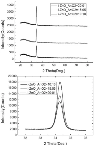
Fig. 7을 토대로 O2/Ar+O2가 transmittance에 상당한 영향을 끼 친다는 것을 알 수 있다. Fig. 8과 Table 6은 film들의 XRD를 측 정한 것이다. Fig. 9에서 보면 34.2°에서 Peak이 관찰 된 것을 알 수 있다. O2/Ar+O2가 증가할수록 peak의 intensity가 감소하게 된다. 이는 Table 6에서의 grain size와 연관 되는 것으로 보인다.
Fig. 8. XRD Patterns of i-ZnO film with various Ar:O2 ratios
Table 6. Analysis results of XRD
i-ZnO (Ar:O2) 2-Theta (Deg.) FWHM Crystal size (Å)
10:10 34.251 0.453 188
15:05 34.258 0.446 191
20:01 34.279 0.437 196
Eff (%) Voc
(V) Jsc
(mA/cm2) FF (%) Rsh
(ohm) Rs
(ohm) Ar:O2=10:10 9.93 0.629 30.96 50.94 495.01 14.33 Ar:O2=15:05 14.99 0.631 34.40 69.06 1855.29 4.23 Ar:O2=20:01 16.35 0.609 36.65 73.29 2796.86 3.72 Fig. 9. Photovoltaic properties of CIGS solar cell with various
Ar:O2 ratios
Fig. 10. Spectral quantum efficiency of CIGS cells with various Ar:O2 ratios
Table 7. Effect of Al thickness on cell performance
Al_400nm Eff (%) Voc
(V) Jsc
(mA/cm2) FF (%) Rsh
(ohm) Rs (ohm)
#1 15.82 0.646 32.67 75.03 23265.43 3.81
#2 15.60 0.622 33.52 74.88 5816.36 3.86
#3 14.73 0.618 33.28 71.66 2585.05 4.98
#4 16.05 0.631 33.32 76.31 11131.79 3.63
#5 16.15 0.623 34.05 76.18 2326.54 3.64 Average 15.67 0.628 33.37 74.81 9025.03 3.98 Al_3um Eff
(%) Voc
(V) Jsc
(mA/cm2) FF (%) Rsh
(ohm) Rs
(ohm)
#6 15.14 0.646 31.03 75.55 3877.57 3.64
#7 14.57 0.617 31.08 75.93 7495.40 3.57
#8 14.48 0.595 32.56 74.81 2498.47 3.57
#9 14.50 0.619 31.36 74.74 4653.09 3.58
#10 14.38 0.586 32.81 74.79 21595.66 3.32 Average 14.61 0.613 31.77 75.16 8024.04 3.54
O2/Ar+O2가 증가할수록 grain size도 감소하게 된다. Fig. 9는 O2/Ar+O2의 ratio에 따라서 Cell을 제작하여서 Photovoltaic properties를 측정한 값이다. 여기서 보면 O2/Ar+O2가 증가할수 록 Series resistance의 값이 증가 하는 것을 알 수 있다. 이는 i-ZnO는 O2/Ar+O2가 증가할수록 resistivity값이 증가 하게 된 것에 기인한 결과 값이라 추측해 볼 수 있다. 또한, O2/Ar+O2가 증가할수록 Current density가 낮아지는 것을 볼 수 있다. 이를 알아보기 위해서 Q.E를 측정하였다. Fig. 10은 Q.E 측정값이다.
여기서 보면 O2/Ar+O2가 증가할수록 Q.E가 전체적으로 떨어지 는 것을 볼 수 있다. 이를 근거로 Current density가 낮아지는 것 을 설명 할 수 있다.
Fig. 11. Best cells with different Al thicknes
Table 8. Effect of Ni interlayer
Al_3um Eff (%) Voc
(V) Jsc
(mA/cm2) FF
(%) Rsh (ohm) Rs
(ohm)
#1 11.28 0.659 24.47 69.95 2012.99 4.72
#2 11.91 0.657 24.71 73.41 2012.99 4.37
#3 11.44 0.654 23.26 75.26 1717.48 4.38
#4 12.18 0.657 24.46 75.76 3019.49 4.31
#5 10.72 0.641 22.52 74.27 2115.04 4.45
#6 10.93 0.655 23.34 71.49 4025.99 4.56 Average 11.41 0.654 23.79 73.36 2484.00 4.46 Ni_50nm
Al_3um Eff (%) Voc
(V) Jsc
(mA/cm2) FF
(%) Rsh
(ohm) Rs
(ohm)
#7 11.93 0.678 24.23 72.54 4174.42 4.79
#8 10.64 0.670 21.18 74.96 24155.97 4.96
#9 10.24 0.665 20.62 74.69 3450.85 5.13
#10 11.94 0.674 23.46 75.47 24155.97 4.44
#11 11.10 0.657 24.32 69.51 8051.99 5.27 Average 11.17 0.669 22.76 73.43 12797.84 4.92
3.3 Al 두께와 nickel 사용에 따른 electrode 층의 특성 변화
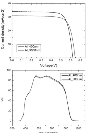
Table 7은 Al을 400 nm와 3 um로 증착 한 cell들의 Pho- tovoltaic properties를 나타낸다. Al의 두께가 증가함에 따라서 Efficiency, open circuit voltage, current density가 떨어지는 것
을 알 수 있다. 이는 3 um로 증착 한 cell의 경우에는 e-beam evaporation되는 과정에서 grid의 폭이 넓어져서 인 것 같다. Fig.
11은 400 nm, 3 um 증착 한 cell중에서 효율이 높았던 것을 비교 한 것이다. 여기서 보면 Al 400 nm인 것이 Al 3 um 보다 Current density가 높은 것을 알 수 있다. 이유를 확인 하기 위해서 QE를 측정해 보았다. QE에서 보면 Al 400 nm로 증착 한 것이 Al 3 um 으로 증착 한 것 보다 전체적으로 QE 값이 증가한 것을 알 수 있 었다.
Table 8은 Al 3 um 증착 시에 Ni layer의 존재 여부에 따른 Photovoltaic properties의 특성을 비교한 것이다. 여기서 보면 Ni layer를 사용한 Cell들의 값의 Open circuit voltage의 값이 증 가 한 것을 알 수 있다. 그러나 Current density가 감소하게 되어 서 효율의 변화가 없었다. Al 증착 시에 Ni를 증착 하면 current 수집과 낮은 resistance를 얻을 수 있다고 알려져 있다15,17,18,19).
4. 결 론
CIGS 태양전지는 다양한 층들이 증착 이 되어진 결과물이다.
이번 실험에서는 태양전지 층들 중에서 ZnO:Al, i-ZnO, electrode 층 들의 변수를 주어서 Photovoltaic properties에 어떠한 영향을 끼치는지에 대해 알아보았다.
ZnO:Al은 Power가 200 W 일 때 resistivity의 값이 작게 나왔 다. 이를 태양전지에 적용한 결과 series resistance의 값 또한 작 아진 것을 확인 할 수 있다. 이는 다른 power에서 증착 하는 것 보 다 좋은 특성을 가지는 Al doped zinc oxide 층을 제작할 수 있을 것이다. 또한 태양전지의 효율을 높이는데도 기여 을 할 것이라 예상한다.
i-ZnO는 O2 pressure가 증가함에 따라서 광학적인 특성이 안 좋아지는 것을 알 수 있다. 이를 태양전지에 적용하여서 Photo- voltaic properties를 관측한 결과에서도 특성들이 안 좋아지는 것을 확인 할 수 있다. 이는 O2 pressure를 증가하는 것은 태양전지 제작에 있어서 효율을 높이는데 부적합 하다는 것을 알 수 있다.
Electrode 층에서의 Al 두께 변화와 Ni층의 유무에 대해서 Photovoltaic properties를 관측 하였다. Al을 3 um까지 증착 시 키는 것과 Ni층을 사용하는 것 이 두 가지의 factor는 효율을 증 가 시키지 못했다. 이는 Al의 3 um 증착과 Ni층의 적용은 부적합 하다는 것을 알 수 있다. 이는 추후에 Al의 두께를 변화 시켜서 최적화 된 것을 찾고, Ni을 적용 한다면 효율을 높이는데 기여 을 할 수 있을 것이라 예상한다.
세 가지의 층들을 변화를 시킴에 따라서 태양전지 특성 변화 에 영향을 끼친다는 것을 알 수 있다. 추후에 세 가지의 층들에 다 른 변수를 주어서 최적화된 조건을 찾는 다면 현재 보다 더 높은 효율을 가지는 태양전지 제작을 할 수 있을 것이라 예상한다.
Acknowledgement
This work was financially supported by the Center for Inorganic Photovoltaic Materials (No. 2012-0001167), funded by the Korea Ministry of Education, Science, and Technology.
References
1. J. N. Alexander, S. Higashiya, D. Caskey Jr, H. Efstathiadis, P.
Haldar, Deposition and characterization of cadmium sulfide (CdS) by chemical bath deposition using an alternative chem- istry cadmium precursor, Solar Engery Mater. Solar Cells, 125, 47-53, 2014.
2. K. Ellmer, Magnetron sputtering of transparent conductive zinc oxide: relation between the sputtering parameters and the electronic properties, J. Phys. D : Appl. Phys, 33, R17-R32, 2000.
3. J. Hu, R.G. Gordon, Textured aluminum-doped zinc oxide thin films from atmospheric pressure chemical-vapor deposi- tion, J. Appl. Phys., 71, 880, 1992.
4. Je-hsiung Lan, Jerzy Kanicki, An Alternative Transparent Conducting Oxide to ITO for the a-Si:H TFT-LCD Applications, 54-57, AMLCDs`95 2nd International Workshop, 1995.
5. S. Ishizuka, K.Sakurai, A. Yamada, K. Matsubara, P. Fons, K.
Iwata, S. Nakamura, Y. Kimura, T. Baba, H. Nakanishi, T.
Kojima, S.Niki, Fabrication of wide-gap Cu(In1-xGaX)Se2
thin film solar cells: a study on the correlation of cell perform- ance with highly resistive i-ZnO layer thickness, Solar Energy Mater. solar cells, 87, 1-4, 541-548, 2005.
6. F. Couzinie-Devy, N.Barreau, J. Kessler, Dependence of ZnO:Al properties on the substrate to target position in RF sputtering, Thin solid Films, 516, 7094-7097, 2008.
7. D.C. Look, Recent advances in ZnO materials and devices, Mater.Sci. Eng, B80, 383, 2001.
8. D. S. Wiersma, The smallest random laser, Nature, 406, 132-133, 2000.
9. P. H. Holloway, T. A. Trottier, B. Abrams, C. Kondoleon, S. L.
Jones, J. S. Sebastian, W. J. Thomes and H. Swart, Advances in field emission displays phosphors, J. Vac. Sci. Techol. B, 17, 758, 1999.
10. H. CaO, J. Y. Xu, D. Z. Zhang, S. H. Chang, S. T. Ho, E. W.
Seelig, X. Liu, and R. P. H. Chang, Spatial confinement of laser light in active random media , Phys. Rev. Lett, 84, 5584-5587,
2000.
11. M.A. Contreras, J.R Tuttle, A. Gabor, A. Tennant, K. Ramanathan, S. Asher, A. Franz, J. Keane, L. Wang, J. Scofield, and R.
Noufi/ High efficiency Cu(In,Ga)Se2-based solar cells: Proc.
novel absorber structures, 68-75, 24th IEEE Photovolt, Special.
Conf., 1994.
12. K. Ramanathan, M. A. Contreras, C. L. Perkins, S. Asher, F. S.
Hasoon, J. Keane, D. Young, M. Romero, W. Metzger, R.
Noufi, J. Ward and A. Duda, Properties of 19.2% Efficiency ZnO/CdS/CuInGaSe2 Thin-film Solar cells, Prog. Photovolt:
Res. Appl, 11, 225-230, 2003.
13. P. Jackson, D. Hariskos, E. Lotter, S. Paetel, R. Wuerz, R.
Menner, W. Wischmann and M. Powalla, New world record efficiency for Cu(In,Ga)Se2 thin-film solar cells beyond 20%, Prog. Photovolt: Res. Appl, 19, 894-897, 2011.
14. O. Cao, O. Gunawan, M. Copel, K. B. Reuter, S. J. chey, V. R.
Deline, and D. B. Mitzi, Defects in Cu(In,Ga)Se2 Chalcopyrite Semiconductors: A Comparative Study of Material Properties, Defect States, and Photovoltaic Performance, Adv. Energy Mater, 1, 845-853, 2011.
15. A. Chirila, P. Bloesch, S. Seyrling, A. Uhi, S. Buecheler, F.
Pianezzi, C. Fella, J. Perrenoud, L. Kranz, R. Verma, D. Guettler, S. Nishiwaki, Y.E. Romanyuk, G.Bilger, D. Bremaud and A.N. Tivari, Cu(In,Ga)Se2 solar cell grown on flexible polymer substrate with efficiency exceeding 17%, Prog. Photovolt: Res.
Appl, 19, 560-564, 2011.
16. P. Reinhard, A. Chirila, F. Pianezzi, S. Nishiwaki, S. Buecheler and A. N. Tivari, High efficiency flexible Cu(In,Ga)Se2 Solar cells, 79-82, AM-FPD 2013 20th International Workshop, 2013.
17. P. Liska, K. R. Thampi, M. Gratzel, D. Bremaud, D. Rudmann, H. M. Upadhyaya, and A. N. Tiwari, Nanocrystalline dye-sen- sitized solar cell/copper indium gallium selenide thin-film tan- dem showing greater than 15% conversion efficiency, Appl.
Phys. Lett., 88, 20310, 2006.
18. M. B. Ard, K. Granath, L. Stolt, Growth of Cu(In,Ga)Se2 thin films by coevaporation using alkaline precursors, Thin Solid Films, 361, 9-16, 2000.
19. Malm U, Edoff M, Influence from front contact sheet resistance on extracted diode parameters in CIGS solar cells, rog. Photovolt:
Res. Appl., 16, 113-121, 2008.
20. Chia-Hua Huang, Hung-Lung Cheng, Wei-En Chang, and Ming-Show Wong, Comprehensive Characterization of DC Sputtered AZO Films for CIGS Photovoltaics, J. Electrochem.
Soc., 158, H510-H515, 2011.