6
Hartley-VCO Using Linear OTA-based Active Inductor
Seong-Ryeol Jeong
*, Won-Sup Chung
*★Abstract
An LC-tuned sinusoidal voltage-controlled oscillator (VCO) using temperature-stable linear operational transconductance amplifiers (OTAs) is presented. Its architecture is based on Hartley oscillator configuration, where the inductor is active one realized with two OTAs and a grounded capacitor. Two diode limiters are used for limiting amplitude. A prototype oscillator built with discrete components exhibits less than 3.1%
nonlinearity in its current-to-frequency transfer characteristic from 1.99 MHz to 39.14 MHz and 220 ppm/ºC frequency stability to the temperature drift over 0 to 75 ºC. The total harmonic distortion (THD) is as low as 4.4 % for a specified frequency-tuning range. The simulated phase noise of the VCO is about -108.9 dBc/Hz at 1 MHz offset frequency in frequency range of 0.4 – 46.97 MHz and property of phase noise of VCO is better than colpitts-VCO.
Key words: Analog Circuit, Hartley oscillator, Voltage-controlled oscillator, OTA, Active Inductor
* Dept. of Semiconductor Engineering, Cheongju University [email protected], 043-229-8462
★ Corresponding author
※ Acknowledgment
This work was supported by the research grant of Cheongju University in 2014. This work was also supported by research scholarship of Cheongju University in 2015-2016.
Manuscript received Agu. 24 2015; revised Oct 21, 2015
; accepted Oct 23. 2015
This is an Open-Access article distributed under the terms of the Creative Commons Attribution Non-Commercial License (http://creativecommons.org/licenses/by-nc/3.0) which permits unrestricted non-commercial use, distribution, and reproduction in any medium, provided the original work is properly cited.
I. Introduction
Voltage (current)-controlled oscillators (VCOs) with sinusoidal outputs have a number of important applications in instrumentation, measurement, and communication systems.
Sinusoidal VCOs with wide sweep capability can be realized by using operational transconductance amplifiers (OTAs) as active components [1]. In these realizations, the
variation of the oscillation frequency is obtained by controlling the transconductance gain of the OTA incorporated in the frequency-determining network. Since the transconductance gain of the OTA can be varied by an external dc bias current, the VCO operation can be readily implemented. The OTA-based VCOs reported so far are generated from four classical oscillator models, namely the phase-shift, the Wien-bridge, the quadrature[2,3,4], and the state-variable bandpass oscillators, These VCOs exhibit relatively wide frequency sweep ranges, but do not provide sufficient frequency stability to use them as a precise component in the design of instrumentation and measurement systems [1].
LC-tuned oscillators have higher frequency stability than RC-active oscillators mentioned above. Therefore, VCOs with higher stability can be generated from LC-tuned oscillator models. LC-tuned VCOs are based on two classical oscillator models: one is based on the positive-feedback LC-tuned oscillator with the 2nd-order loop gain (namely LC-bandpass
oscillator), the other on the negative-feedback one with the 3rdorder loop gain (namely Colpitts and Hartley oscillator). VCOs based on the former LC-bandpass oscillator is reported in [5][6].
In these VCOs, the inductor is active one by interconnecting two matched OTAs and a grounded capacitor, and the resultant equivalent inductance is inversely proportional to the square of the transconductance gain of OTAs.
The active inductor in turn together with a capacitor forms a LC resonant circuit to determine the oscillation frequency. A main disadvantage of the LC-bandpass VCOs is their relatively poor frequency stability with regard to temperature. This arises from the fact that the VCOs employ nonlinear OTAs as active elements. The nonlinear OTAs usually have the transconductance gain which is dependent on temperature as well as bias current, and hence the VCOs implemented with these devices are sensitive to temperature. The difficulty in maintaining the amplitude of oscillation to be constant over a wide frequency range without loop gain adjustment is another disadvantage of the LC-bandpass VCOs [7][8].
In this paper an LC-tuned VCO, based on Hartley oscillator, with excellent frequency stability is presented. These improved performances are achieved by introducing a lightly linear and temperature-stable OTA into the oscillator circuit and making them operate within their input linear ranges [6].
II. Architecture
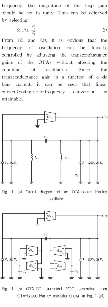
Fig. 1(a) shows the circuit diagram of an OTA-based Hartley oscillator. It consists of a 3rd-order LC-tuned circuit connected in a negative-feedback loop with an OTA and two diode limiters. To understand how this circuit works, assume that oscillations have already
started. The output of the tuned circuit will be a sine wave whose frequency is equal to the center frequency of the tuned circuit,
. The sine wave voltage signal is fed to the OTA, and converted into a current signal whose value is equal to the product of the signal voltage by a transconductance gain of the OTA. This sine wave current signal is limited by the diode limiter, and in turn is fed to the LC-tuned circuit, which filters out the harmonics and provides a sinusoidal output voltage at the fundamental frequency. The purity of the sine wave is determined by the selectivity of the LC-tuned circuit, whose control is achieved by way of the resistance R. To sustain oscillations, the magnitude of the loop gain is made greater than unity. Fig. 1 (b) shows an OTA-RC sinusoidal VCO generated from the basic configuration of the OTA-based Hartley oscillator shown in Fig. 1 (a). In Fig. 1 (b), left two identical OTAs marked and a grounded capacitor form one grounded inductor and right two identical OTAs and a grounded capacitor form the other grounded inductor, whose equivalent inductance is
and . Disregarding the limiter circuit and assuming ideal OTAs, the loop gain of the oscillator circuit given by
(1)
where is transconductance gain of the ith OTA.
If , the phase of the loop gain will be zero at one frequency given by
(2)
To obtain sustained oscillations at this frequency, the magnitude of the loop gain should be set to unity. This can be achieved by selecting
≥
(3) From (2) and (3), it is obvious that the frequency of oscillation can be linearly controlled by adjusting the transconductance gains of the OTAs without affecting the condition of oscillation. Since the transconductance gain is a function of a dc bias current, it can be seen that linear current(voltage)-to-frequency conversion is attainable.
Fig. 1. (a) Circuit diagram of an OTA-based Hartley oscillator.
Fig. 1. (b) OTA-RC sinusoidal VCO generated from OTA-based Hartley oscillator shown in Fig. 1 (a).
III. Temperature-stable linear OTA
A circuit diagram of a new temperature-stable linear OTA designed for the Colpitts VCO is shown in Fig. 2 [9]. It consists of a linear transconductor formed by transistors - and an emitter-degeneration resistor , a translinear current gain cell -, and three Wilson current mirrors -. The transconductor converts the differential input voltage to its corresponding differential output currents and . Its operation can be explained as follows: For simplicity, we assume that all transistors are identical. Since the base-emitter junctions of and are connected in parallel with those of and , respectively, we can write
and . The collector current is reproduced at the emitter of through the current mirror, formed by and , to bias
. In the same manner, is biased by the collector current which is reproduced at the emitter of through the current mirror formed by and . Summing the voltages around the loop consisting of the input voltage source, the four base-emitter junctions of , and the emitter degeneration resistor , we obtain
ln
ln
ln
ln
(4)
Where is the thermal voltage, and are the common-base current gain and saturation current of the pnp transistors, respectively, and
is the saturation current of the npn transistors. Since
(5a)
(5b)
(4) can be rewritten as follows:
ln
ln
ln
ln
(6)
Where is the common-emitter current gain of the pnp transistors. The sum of the terms including is zero, and hence (6) reduces to
(7)
Since the sum of and is , and
will be given by
(8a)
(8b)
The differential output currents , of the transconductor drive the diode-connected transistor pair and of the translinear current gain cell. The current gain cell makes the current partitioning of the transistor pair
and to be the mirror image of the current partitioning of the transistor pair and . Therefore, we can write the following relation:
(9)
The output currents and of the current gain cell are differenced by three current mirrors formed by -, -, and -, respectively. Since the sum of and is
and the difference is , which denotes the single-ended output current of the OTA, currents and can be written as follows:
(10a)
(10b)
Combining (8a), (8b), (10a), and (10b) into (9),
one can obtain the transfer function of the OTA expressed as follows:
(11)
The transconductance gain is given by (
). It should be noted that in deriving (11) base-width modulation effect of transistors was not considered. Also, note that the transconductance gain of the OTA is determined by the ratio of the dc bias currents
and . DC current sources for and
consist of a simple current mirror and a resistor, respectively. SPICE simulation using HFA3096 transistor arrays shows that temperature coefficient (TC) of / current ratio is less than 120 ppm/℃ in a temperature range of 0–75℃. Resistors and used for the OTA are precision ones having TC of 50 ppm/℃ and tolarance of ±0.05%.
The discussion up to now has not considered the base-width modulation effect of transistors.
However, in reality, nonideality due to the base-width modulation effect is present. The influence of the base-width modulation effect of transistors on the transfer characteristic of the OTA is mainly caused by the changes in of
, and of , . Considering the basewidth modulation effect of transistors, (11) may be modified to
(12)
Where and are the Early voltages for the pnp and the npn transistors, respectively.
, and , would be influenced by supply voltage variation. SPICE simulation shows that varying supply voltages from = 3V and = to = 3V±0.5V and =
∓0.5V, respectively, variation in is about −1.4 ppm/V. Hence the dependency of
on (or ) can be neglected.
It can be shown from (8a) and (8b) that the input linear range of the OTA is
≤ (13)
From (2) and (11), it is obvious that the Hartley VCO of Fig. 1 (b) implemented with this OTA oscillates at the frequency given by
(14)Also, from (3) and (11), it can be seen that the condition of oscillation is given by
≥
(15)
where denotes bias current of OTA5.
Fig. 2. Circuit diagram of a temperature-stable linear OTA
Ⅳ. Experimental Results
A breadboard prototype of Fig. 1 (b) has been devised using the OTA shown in Fig. 2 and polystyrene capacitors. The transistor arrays used for the OTA were HFA3096. The resistors were = 1 kΩ and = 1 kΩ. The bias current was set to 1 mA to obtain a input linear range of ± 1 V. All measurements
were performed at supply voltages of = -
= 3V. The relation between the frequency of oscillation and the bias current was measured with = = 8 pF, = 1 pF, R
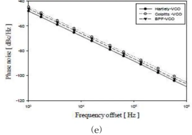
= 1 kΩ, and = 1 mA. The results are plotted in Fig. 3 (a), which shows that the frequency of oscillation can be linearly controlled by the bias current over the frequency range of 3.17 to 30.56 MHz with the linearity error less than 3.1% over the bias current range of 150 to 1500 μA. In this condition, the transfer rate of the dc bias current to the oscillation frequency is 20 kHz per a unit μA. The maximum frequency range is from 400 kHz to 46.97 MHz. For comparison, the relations between the frequency and the bias current obtained by the conventional bandpass-filter (BPF)-based VCO in [6] and Colpitts VCO in [1] are also shown in Fig. 3 (a). The temperature stability of the oscillator frequency measured over the range of 0 to 75 ℃ is plotted in Fig. 3 (b) with the broken line, indicating that the temperature drift is less than 220 ppm/℃ over the frequency range of 0.96 to 42.62 MHz. This drift is about 4.5 times lower than that of the previous work described in [9] and about two times higher than that of the Colpitts VCO in [1].
The peak-to-peak amplitude of the output sine wave measured over the same bias current range is plotted in Fig. 3 (c). The amplitude is relatively stable up to 0.9V. The total harmonic distortions (THDs) of the output sine waves for each VCO are plotted in Fig. 3 (d), indicating that the THD is as low as 4.4 percent over the bias current range of 500 to 2000μA, while the THD of the Hartley VCO is about two times higher than that of the Colpitts VCO. Comparing Fig. 3 (a), (b), (c) and (d), the frequency stability is excellently maintained in the range that peak-to-peak amplitude is relatively stable. It shows that the diode limiters is related to the frequency
(a)
(b)
(c)
(d)
(e)
Fig. 3 (a) Measured frequency of oscillation against the bias current for each VCO, (b) Measured temperature stability of frequency for each VCO, (c) Peak-to-peak amplitude, (d) Measured THD of the output sine wave for each VCO, (e) Phase
noise of each VCO
stability. The phase noise of the VCO was simulated by using the Spectre RF advanced PSS and Pnoise analysis. The result is shown in Fig. 3 (e), indicating that the phase noise of the VCO is about 108.9dBc/Hz at 1 MHz offset frequency. Fig. 3 (e) also shows that the phase noise of the proposed oscillator is about 3.7dB lower than that of the Colpitts VCO, and is about 2.1dB lower than that of the BPF-based VCO.
V. Conclusions
A new OTA-based sinusoidal Hartley-VCO using temperature stable linear OTAs as active devices has been described. It can linearly control its frequency by adjusting a dc bias current and it exhibits excellent frequency stability over a tuning range. It can be used as a current to frequency converter due to its high transfer rate of the dc bias current to the oscillation frequency. Thus, the proposed oscillator can be used for implementing the precise instrument systems without being affected by temperature drift or the local oscillator in the communication systems. The
proposed oscillator architecture has potential to operate at much higher frequencies by using an OTA implemented with a high-frequency bipolar transistor technology. Two diode limiters for limiting the amplitude of the oscillation can be replaced by the automatic gain control (AGC) circuit.
References
[1] W.-S. Chung, S.-H. Son, and H.-S. Kim,
"Colpitts VCO Using Temperature-Stable
Linear OTAs", IEICE Electron. Express, Vol.
10, No.13, pp. 1-9, July 2013.
[2] A. Jannesari and M. Kamarei, "Sinusoidal- Switched Serial-Coupled CMOS LC quadrature VCO", IEICE Electronics Express, Vol. 4, No.
13, pp.423-429, July 2007.
[3] J. Chang and C. K. Kim, "A Symmetrical 6-GHz fully integrated Cascode coupling CMOS LC quadrature VCO", IEEE Microw. Wireless Compon. Lett., Vol. 15, No. 10, pp. 670-672, Oct. 2005.
[4] H. Choi, S. B. Shin, and S. Lee, "A Low-phase noise LC-QVCO in CMOS technology", IEEE Microw. Wireless Compon.
Lett., Vol. 14, No. 11, pp. 540-542, Nov. 2004.
[5] H. Kim, W.-S. Chung, J.-M. Park, S.-H.
Son, "A LC-Tuned Sinusoidal VCOs Using OTA-C Active Inductors", ITC-CSCC, Vol.
2004, No.7, pp. 3-6, July 2004.
[6] H. Kim, J.-W. Kim, W.-S. Chung, J.-M Park and H.-J. Kim, "A LC-Tuned Sinusoidal VCO Using Temperature-Stable Linear OTAs", ITC-CSCC 2003 Proceedings,Vol. 26, pp. 601–
04, July 2003.
[7] Prabir C. Maulik and Ping Wing Lai,
"Frequency Tuning of Wide Tempe-rature Range CMOS LC VCOs", IEEE JOURNAL OF SOLID-STATE CIRCUITS, Vol.46, No.9, pp.2033-2040, Sep. 2011.
[8] W.-S. Chung and K. Watanabe, "A temperature difference-to-frequency converter using resistance temperature detectors", IEEE Trans. Instrum. Meas., Vol. IM-39, pp. 676-677, Aug. 1990.
[9] W-S Chung, S-H Son, "Semiconductor and devices", Journal of the Institute of Electronics Engineers of Korea, Vol. 44, No. 7, pp. 37-44, 2007.
BIOGRAPHY
Seong-Ryeol Jeong (Student Member) 2015 : BS degree in Semi- conductor Engineering, Cheongju University.
2015~Present : He is studying a MS degree in Semiconductor Engineering,
Cheongju University.
Won-Sup Chung (Member)
1977 : BS degree in Electrical Communication Engineering, Hanyang University.
1979 : MS degree in Electrical Communication Engineering, Hanyang University.
1986 : PhD degree in Electrical Science Engineering, Shizuoka University.
1986~Present : Professor in Department of Semiconductor Engineering, Cheongju University.