밀리미터파 응용을 위해 Radial 프로브
마이크로 스트립-웨이브 가이드 광대역 천이기
(Wide Band Microstrip line-to-Rectangular Waveguide Transition Using a Radial Probe for Millimeter-wave
Applications)
이 영 철1)*
(Young Chul Lee)
요 약 본 논문에서는 밀리미터파 모듈 응용을 위하여 광대역 마이크로스트립-대-웨이브가이 드 (WR12) 천이기가 제시된다. 대역폭의 개선을 위하여 radial 마이크로 스트립 electrical-probe 가 저 손실 유기 유전체 기판 위에 설계되었다. 제안된 천이기의 삽입 및 반사손실에 대한 설계 및 측정된 특성을 나타내었다. 측정을 위한 케이블 아답터와 웨이브가이드 천이기의 손실을 고려 하면, 제안된 천이기의 천이 손실이 70 및 80 GHz에서 각각 –1.88 및 –2.01 dB로 분석되었다.
제안된 천이기의 -10 dB 반사 손실 대역폭은 67GHz 에서 95 GHz로 약 26 GHz이다. 최신의 연 구결과와 비교해서 대역폭에서 8.3 % 개선되었다.
핵심주제어 : 천이기, 마이크로스트립, WR12, 웨이브가이드, E-band
Abstract In this work, a broadband microstrip (MSL) - to - waveguide (WR12) transition has been presented for millimeter-wave module applications. For improvement of a bandwidth, the radial MSL electrical-probe is designed on the low-loss organic dielectric substrate. The designed and tested characteristics of the proposed transition are characterized in terms of an insertion and return loss. Considering the loss contribution of the cable adapter and waveguide transition for the measurement, the proposed transition loss can be analyzed as –1.88 and –2.01 dB per a transition at 70 and 80 GHz, respectively. The bandwidth of the proposed transition for reflection at -10 dB is 26 GHz at all test frequencies from 67 to 95 GHz. Compared to the state-of-the-art results, improvement of 8.3
% is achieved for the operation bandwidth.
Key Words : Transition, Microstrip, WR12, Wavguide, E-band
1. Introduction
* Corresponding Auther : [email protected]
Manuscript December 10, 2014 / Revised February 06, 2015 / Accepted December 16, 2015
1) 목포해양대학교 전자공학과, 제1저자
Recently, because of high demands for several ultra high-data-rate wireless, millimeter-wave (mm-wave) frequency band for services has been increased to Ka-band, V-band, and E-band.
Especially, 71 ~ 76 and 81 ~ 86 GHz bands known as "E-band" are widely permitted around the world
for ultra high-capacity point-to-point wireless communications applications[1]. E-band wireless systems offer the most competitive alternative to Ka-band and V-band systems and buried fiber because of very wide available bandwidth (BW) of 10 GHz, low-loss propagation characteristics in free space, and cost effective solution in terms of license and installation.
In general, mm-wave devices, components, and modules are designed using several technologies and materials. Therefore, they are integrated and assembled in the system each other by using various transmission lines; microstrip line, coplanar line, waveguides et al..
Therefore, a low-loss transition between them is one of key elements in the mm-wave system design. In nature, simple design, wide bandwidth, and low loss are key issues for mm-wave system applications.
A popular electrical-probe (E-probe) transition [2] with a back-short waveguide on the dielectric substrate has been used because of its simple mode transformation and easy design, compared to other perpendicular transitions [3-5] and also no additional substrate is required. However, narrow operation bandwidth is the essential drawback.
For broad bandwidth applications, a waveguide transition using a quasi-Yagi Uda antenna printed on the substrate was proposed [6], but in addition, air bridges and a trenched metal block were needed. A very wide bandwidth of 24.9 GHz was achieved [7] by controlling the position of the probe and length of an extended ground (GND) [8]
related to the reactance of the probe.
The dielectric material as well as the transition structures should be considered for low-loss transition design. In general, RT/Duroid 5880 [3,4,7,9] and low- temperature co-fired ceramic (LTCC) [5,10] as a substrate have been frequently used for mm-wave applications, because of a very small loss tangent and low coefficient of thermal expansion (CTE). Considering integration into inner
layers of printed circuit boards (PCBs), low-loss organic material; Liquid Crystalline Polymer (LCP) has been utilized for microwave and mm-wave module applications [11].
In this work, a wide band microstrip-to -waveguide (MSL-to-WG) transition has been presented for E-band applications. For wide operational bandwidth, simple radial probe is designed on the LCP organic dielectric substrate.
The designed and measured results of the proposed transition are characterized in terms of an insertion and return loss.
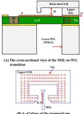
(A) The cross sectional view of the MSL-to-WG transition
Via
(B) A-A?plane of the proposed one
Upper GND
IL1 MSL
A H
LCP
Back-short Lid
Lower WG (WR12)
Upper WG
Via A?
RF IC
Fig. 1 Configuration of a MSL-to- WR12 transition.
2. Design of a MSL-to-WR12 Transition
The transitions were designed and analyzed by using a 3-D Finite Integration Technique (FIT) simulator. A relative dielectric constant, loss tangent, and height of the LCP substrate are 3.16, 0.0045, and 100 μm, respectively at 70 GHz and metal (Cu) patterns on the substrate is 8 μm thick.Fig. 1 shows the cross-sectional view of the proposed MSL-to-WG transition. A MSL-to- WG transition is composed of a rectangular open-ended WG, short-circuit WG, and LCP dielectric substrate with he radial electrical probe. The probe and GND patterns are designed on the both side of the substrate. Via holes are formed around WG in the LCP substrate. For 70 and 80 GHz applications, WR12 WG was used and its rectangular size is 3.1 mm x 1.55 mm. The LCP dielectric substrate is placed on the open-ended WR12 (lower WG) and then the short-circuited WG is on it as shown in Fig. 1 (A). Conductor patterns on the LCP substrate is designed as shown in Fig. 1 (B). A length (H) of the short-circuit WG is a quarter of guided wavelength of the WG (λg/4), in order to couple electric current on the probe to TE10 dominant mode of the WG. For suppression of parallel-plate leakage (PPL) in the LCP substrate, vias are placed as shown in Fig. 1 (B). In order to achieve a wide-band impedance matching, the extended GND and radial patch are designed as shown in
<Fig. 1 (B)>. The length and angle of the radial probe are 0.321 mm and 900, respectively. They were optimized for broadband characteristics of the transition. Narrow MSL between the MSL and radial probe is designed for impedance matching.
Its width and length are 0.11 and 1.184 mm, respectively. The Width of the 50-Ω MSL is 0.236 mm. In order to evaluate the transitions, they were designed in a back-to-back structure and length between two transitions was 20.6 mm.
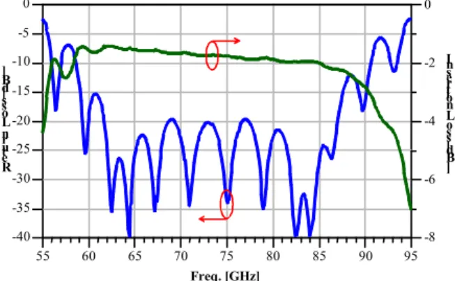
The simulated results of the proposed transition are presented in Fig. 2. Its BW of the proposed transition for reflection at -20 dB is 25.5 GHz (34.34 %) from 61.5 to 87 GHz. An insertion loss is –1.67 and –1.95 dB at 70 and 80 GHz, respectively.
60 65 70 75 80 85 90
55 95
-35 -30 -25 -20 -15 -10 -5
-40 0
-6 -4 -2
-8 0
Freq. [GHz]
Ret urn L oss [d
B] In
sert ion Lo ss [d B]
Fig. 2 Simulated results of the proposed transition.
3. Fabrication and Measurement of the MSL-to-WR12 Transition
The designed transitions were fabricated in a commercial printed circuit board (PCB) foundry.
Fig. 3 shows the fabricated transitions on the LCP substrate in a back-to-back structure.
Fig. 3 Fabricated transitions in a back-to-back structure.
For the test, the fabricated LCP substrate including transition patterns is attached on the lower WR12 in aluminium (Al) block by using a conductive epoxy. The upper WR12 and back-circuit cover are placed on the substrate in order. All parts are tightened by screws.By using a vector network analyzer (VNA) the fabricated back-to-back transition were tested. After calibration, adapters (1.0 mm male cable-to-WR10) and WG transitions (WR10-to-WR12) were
connected to the cable of the VNA. Fig. 4 presents a photograph of device under test (DUT) for the fabricated board including several transitions. The test frequency was from 67 to 95 GHz.
Fig. 4 Test set-up of the fabricated transition [Two W-band adapters and waveguide transitions are used for test].
70 75 80 85 90
65 95
-30 -20 -10
-40 0
-35 -25 -15
-45 -5
Freq. [GHz]
Ret urn L oss [d
B] In
sert ion Lo ss [d B]
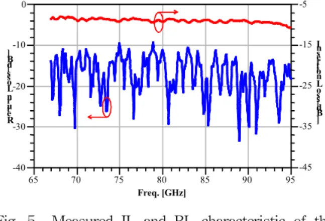
Fig. 5 Measured IL and RL characteristic of the fabricated transition.
Fig. 5 presents the measured insertion loss (IL) and return loss (RL) of the fabricated transition in the back-to-back structure. All test results are degraded compared to the simulated ones because of high-loss calibration using several adapters and WG transitions. The RL of the proposed transition shows less than -10 dB at all test frequencies.
The IL of -8.9 and –9.2 dB is obtained at 70 and 80 GHz, respectively. This IL includes the loss portion of the long MSL, W-band adapter, and WG transition. The loss including the 20.6 mm long MSL, adapters, and WG transitions is -5.14 and –5.18 dB, 70 and 80 GHz, respectively.
Considering the loss contribution, the transition loss is analyzed as -1.88 and -2.01 dB per a transition at 70 and 80 GHz, respectively.
4. Conclusion
A wide-band microstrip (MSL) - to - waveguide transition has been presented for millimeter-wave applications. In order to improve its operational bandwidth, the radial MSL probe is designed on the low-loss organic dielectric substrate. Considering the loss contribution of the cable adapter and waveguide transition for the measurement, the proposed transition loss can be analyzed as -1.88 and –2.01 dB per a transition at 70 and 80 GHz, respectively. Its operational bandwidth of 26 GHz is obtained for reflection at –10 dB. Compared to the state-of-the-art results of 24 GHz, the improvement of 8.3 % is achieved.
References
[1] Val Dyadyuk, Y. Jay Guo and John D. Bunton:
“Enabling Technologies for Multi-Gigabit Wireless Communications in the E-Band, Mobile and Wireless Communications Network Layer and Circuit Level Design,” Salma Ait Fares and Fumiyuki Adachi (Ed.), ISBN:
978-953-307-042-1, InTech, Available from:
http://www.intechopen.com/books/mobile-and-wi reless-communications-network-layer-and-circu it-leveldesign/, pp.263-280, 2010.
[2] Shih, Y.-C., Ton, T.-N., and Bui, L.Q.:
“Waveguide-to-microstrip transitions for millimeter-wave applications,” IEEE MTT-s International Microwave Symposium Digest, pp.473-475, 1988.
[3] H. Aliakbarian, A. Enayati, G. A. E.
Vandenbosch, and W. De Raedt: “Novel Low-Cost End-Wall Microstrip -to-Waveguide
Splitter Transition,” Progress In Electromagnetics Research, PIER 101, pp.75-96, 2010.
[4] Jun Dong1, Tao Yang1, Yu Liu1, Ziqiang Yang, and Yihong Zhou: “Broadband Rectangular Waveguide to GCPW Transition,” Progress In Electromagnetics Research Letters, Vol. 46, pp.107-112, 2014.
[5] Simon, W., Werthen, M., Wolff, I.: “A novel coplanar transmission line to rectangular waveguide transition” IEEE MTT-S International Microwave Symposium Digest, Vol. 1, pp.257-260, 1998.
[6] Kaneda, N., Yongxi Qian, and Itoh, T.: “A broad-band microstrip-to-waveguide transition using quasi-Yagi antenna,” IEEE Transactions on Microwave Theory and Techniques, Vol. 47, pp2562–2567, 1999.
[7] Sakakibara, K., Hirono, M., Kikuma, N., Hirayama, H.: “Broadband and planar microstrip- to-waveguide transitions in millimeter-wave band,” International Conference on Microwave and Millimeter Wave Technology (ICMMT), Vol. 3, pp.1278–1281, 2008.
[8] Marcuvitz, N.: Waveguide Handbook, London, U.K.: IEE Press, 1993.
[9] http://www.rogerscorp.com.
[10] Young Chul Lee, “Compact LTCC Patch Antenna Integrating a Wideband Vertical Transition for millimeter-wave SoP Applications,” Journal of the Korea Industrial Information Systems Research Vol. 19 No.1, pp.19-24, 2014.
[11] Young Chul Lee: “70 GHz Tx and Rx LCP SoP Module for Point-to-point Millimetre Wave Applications,” PIERS Proceedings, pp.12-15, 2013.
이 영 철 (Young Chul Lee)
∙정회원
∙영남대학교 전자공학과 공학학사
∙영남대학교 전자공학과 공학석사
∙한국과학기술원 공학부 공학박사
∙목포해양대학교 해양공과대학 전자공학과 부교수
∙관심분야 : 밀리미터파 회로 및 시스템