DM7446A, DM5447A/DM7447A BCD to 7-Segment Decoders/Drivers
June 1989
DM7446A, DM5447A/DM7447A
BCD to 7-Segment Decoders/Drivers
General Description
The 46A and 47A feature active-low outputs designed for driving common-anode LEDs or incandescent indicators di- rectly. All of the circuits have full ripple-blanking input/out- put controls and a lamp test input. Segment identification and resultant displays are shown on a following page. Dis- play patterns for BCD input counts above nine are unique symbols to authenticate input conditions.
All of the circuits incorporate automatic leading and/or trail- ing-edge, zero-blanking control (RBI and RBO). Lamp test (LT) of these devices may be performed at any time when the BI/RBO node is at a high logic level. All types contain
an overriding blanking input (BI) which can be used to con- trol the lamp intensity (by pulsing) or to inhibit the outputs.
Features
Y All circuit types feature lamp intensity modulation capability
Y Open-collector outputs drive indicators directly
Y Lamp-test provision
Y Leading/trailing zero suppression
Connection Diagram
Dual-In-Line Package
TL/F/6518 – 1
Order Number DM5447AJ, DM7446AN or DM7447AN See NS Package Number J16A or N16E
Absolute Maximum Ratings
(Note) If Military/Aerospace specified devices are required, please contact the National Semiconductor Sales Office/Distributors for availability and specifications.Supply Voltage 7V
Input Voltage 5.5V
Operating Free Air Temperature Range
DM54 b55§C toa125§C
DM74 0§C toa70§C
Storage Temperature Range b65§C toa150§C
Note:The ‘‘Absolute Maximum Ratings’’ are those values beyond which the safety of the device cannot be guaran- teed. The device should not be operated at these limits. The parametric values defined in the ‘‘Electrical Characteristics’’
table are not guaranteed at the absolute maximum ratings.
The ‘‘Recommended Operating Conditions’’ table will define the conditions for actual device operation.
Recommended Operating Conditions
Symbol Parameter DM7446A
Units
Min Nom Max
VCC Supply Voltage 4.75 5 5.25 V
VIH High Level Input Voltage 2 V
VIL Low Level Input Voltage 0.8 V
VOH High Level Output Voltage (a thru g) 30 V
IOH High Level Output Current (BI/RBO) b0.2 mA
IOL Low Level Output Current (a thru g) 40 mA
IOL Low Level Output Current (BI/RBO) 8 mA
TA Free Air Operating Temperature 0 70 §C
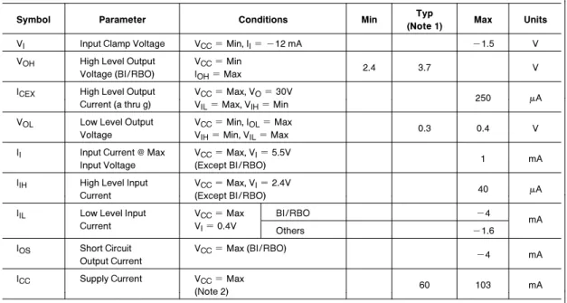
’46A Electrical Characteristics
over recommended operating free air temperature range (unless otherwise noted)
Symbol Parameter Conditions Min Typ
Max Units
(Note 1)
VI Input Clamp Voltage VCCeMin, IIe b12 mA b1.5 V
VOH High Level Output VCCeMin
2.4 3.7 V
Voltage (BI/RBO) IOHeMax
ICEX High Level Output VCCeMax, VOe30V
250 mA
Current (a thru g) VILeMax, VIHeMin VOL Low Level Output VCCeMin, IOLeMax
0.3 0.4 V
Voltage VIHeMin, VILeMax II Input Current@Max VCCeMax, VIe5.5V
1 mA
Input Voltage (Except BI/RBO) IIH High Level Input VCCeMax, VIe2.4V
40 mA
Current (Except BI/RBO)
IIL Low Level Input VCCeMax BI/RBO b4
Current VIe0.4V Others b1.6 mA
IOS Short Circuit VCCeMax (BI/RBO)
b4 mA Output Current
ICC Supply Current VCCeMax
60 103 mA
(Note 2) Note 1:All typicals are at VCCe5V, TAe25§C.
Note 2:ICCis measured with all outputs open and all inputs at 4.5V.
’46A Switching Characteristics
at VCCe5V and TAe25§C (See Section 1 for Test Waveforms and Output Load)
Symbol Parameter Conditions Min Max Units
tPLH Propagation Delay Time CLe15 pF
100 ns
Low to High Level Output RLe120X tPHL Propagation Delay Time
100 ns
High to Low Level Output
Recommended Operating Conditions
Symbol Parameter DM5447A DM7447A
Units
Min Nom Max Min Nom Max
VCC Supply Voltage 4.5 5 5.5 4.75 5 5.25 V
VIH High Level Input Voltage 2 2 V
VIL Low Level Input Voltage 0.8 0.8 V
VOH High Level Output
15 15 V
Voltage (a thru g)
IOH High Level Output b
0.2 b0.2 mA
Current (BI/RBO) IOL Low Level Output
40 40 mA
Current (a thru g) IOL Low Level Output
8 8 mA
Current (BI/RBO)
TA Free Air Operating Temperature b55 125 0 70 §C
’47A Electrical Characteristics
over recommended operating free air temperature range (unless otherwise noted)
Symbol Parameter Conditions Min Typ
Max Units
(Note 1)
VI Input Clamp Voltage VCCeMin, IIe b12 mA b1.5 V
VOH High Level Output VCCeMin
2.4 3.7 V
Voltage (BI/RBO) IOHeMax
ICEX High Level Output VCCeMax, VOe15V
250 mA
Current (a thru g) VILeMax, VIHeMin VOL Low Level Output VCCeMin, IOLeMax
0.3 0.4 V
Voltage VIHeMin, VILeMax
II Input Current@Max VCCeMax, VIe5.5V
1 mA
Input Voltage
IIH High Level Input Current VCCeMax, VIe2.4V 40 mA
IIL Low Level Input VCCeMax BI/RBO b4
Current VIe0.4V Others b1.6 mA
IOS Short Circuit VCCeMax (BI/RBO) b
4 mA
Output Current
ICC Supply Current VCCeMax DM54 60 85
(Note 2) DM74 60 103 mA
Note 1:All typicals are at VCCe5V, TAe25§C.
Note 2:I is measured with all outputs open and all inputs at 4.5V.
’47A Switching Characteristics
at VCCe5V and TAe25§C (See Section 1 for Test Waveforms and Output Load)
Symbol Parameter Conditions Min Max Units
tPLH Propagation Delay Time CLe15 pF
100 ns
Low to High Level Output RLe120X tPHL Propagation Delay Time
100 ns
High to Low Level Output
Function Table
46A, 47A
Decimal or Inputs BI/RBO Outputs
Function LT RBI D C B A (Note 1) a b c d e f g Note
0 H H L L L L H L L L L L L H
1 H X L L L H H H L L H H H H
2 H X L L H L H L L H L L H L
3 H X L L H H H L L L L H H L
4 H X L H L L H H L L H H L L
5 H X L H L H H L H L L H L L
6 H X L H H L H H H L L L L L
7 H X L H H H H L L L H H H H
(2)
8 H X H L L L H L L L L L L L
9 H X H L L H H L L L H H L L
10 H X H L H L H H H H L L H L
11 H X H L H H H H H L L H H L
12 H X H H L L H H L H H H L L
13 H X H H L H H L H H L H L L
14 H X H H H L H H H H L L L L
15 H X H H H H H H H H H H H H
BI X X X X X X L H H H H H H H (3)
RBI H L L L L L L H H H H H H H (4)
LT L X X X X X H L L L L L L L (5)
Note 1:BI/RBO is a wire-AND logic serving as blanking input (BI) and/or ripple-blanking output (RBO).
Note 2:The blanking input (BI) must be open or held at a high logic level when output functions 0 through 15 are desired. The ripple-blanking input (RBI) must be open or high if blanking of a decimal zero is not desired.
Note 3:When a low logic level is applied directly to the blanking input (BI), all segment outputs are high regardless of the level of any other input.
Note 4:When ripple-blanking input (RBI) and inputs A, B, C, and D are at a low level with the lamp test input high, all segment outputs go H and the ripple- blanking output (RBO) goes to a low level (response condition).
Note 5:When the blanking input/ripple-blanking output (BI/RBO) is open or held high and a low is applied to the lamp-test input, all segment outputs are L . HeHigh level, LeLow level, XeDon’t Care
Logic Diagram
TL/F/6518 – 2
Physical Dimensions
inches (millimeters)16-Lead Ceramic Dual-In-Line Package (J) Order Number DM5447AJ NS Package Number J16A
DM7446A, DM5447A/DM7447A BCD to 7-Segment Decoders/Drivers
Physical Dimensions
inches (millimeters) (Continued)16-Lead Molded Dual-In-Line Package (N) Order Number DM7446AN or DM7447AN
NS Package Number N16E
LIFE SUPPORT POLICY
NATIONAL’S PRODUCTS ARE NOT AUTHORIZED FOR USE AS CRITICAL COMPONENTS IN LIFE SUPPORT DEVICES OR SYSTEMS WITHOUT THE EXPRESS WRITTEN APPROVAL OF THE PRESIDENT OF NATIONAL SEMICONDUCTOR CORPORATION. As used herein:
1. Life support devices or systems are devices or 2. A critical component is any component of a life systems which, (a) are intended for surgical implant support device or system whose failure to perform can into the body, or (b) support or sustain life, and whose be reasonably expected to cause the failure of the life failure to perform, when properly used in accordance support device or system, or to affect its safety or with instructions for use provided in the labeling, can effectiveness.
be reasonably expected to result in a significant injury to the user.
National Semiconductor National Semiconductor National Semiconductor National Semiconductor
Corporation Europe Hong Kong Ltd. Japan Ltd.
1111 West Bardin Road Fax: (a49) 0-180-530 85 86 13th Floor, Straight Block, Tel: 81-043-299-2309 Arlington, TX 76017 Email: cnjwge@tevm2.nsc.com Ocean Centre, 5 Canton Rd. Fax: 81-043-299-2408