• 검색 결과가 없습니다.

Fabrication of 1D Metal Oxide Nanostructures Using Glancing Angle Deposition for High Performance Gas Sensors

N/A
N/A
Protected

Academic year: 2021

Share "Fabrication of 1D Metal Oxide Nanostructures Using Glancing Angle Deposition for High Performance Gas Sensors"

Copied!
7
0
0

로드 중.... (전체 텍스트 보기)

전체 글

(1)

http://dx.doi.org/10.5369/JSST.2017.26.4.228 pISSN 1225-5475/eISSN 2093-7563

Fabrication of 1D Metal Oxide Nanostructures Using Glancing Angle Deposition for High Performance Gas Sensors

Jun Min Suh and Ho Won Jang

+

Abstract

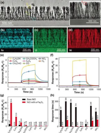
Gas sensors based on metal-oxide-semiconductors are predominantly used in numerous applications including monitoring indoor air quality and detecting harmful substances such as volatile organic compounds. Nanostructures, e.g., nanoparticles, nanotubes, nano- domes, or nanofibers, have been widely utilized to improve the gas sensing properties of metal-oxide-semiconductors by increasing the effective surface area participating in the surface reaction with target gas molecules. Recently, 1-dimensional (1D) metal oxide nano- structures fabricated using glancing angle deposition (GAD) method with e-beam evaporation have been widely employed to increase the surface-to-volume ratio significantly with large-area uniformity and reproducibility, leading to promising gas sensing properties.

Herein, we provide a brief overview of 1D metal oxide nanostructures fabricated using GAD and their gas sensing properties in terms of fabrication methods, morphologies, and additives. Moreover, the gas sensing mechanisms and perspectives are presented.

Keywords: Gas sensors, Metal oxides, Glancing angle deposition, Nanostructures, E-beam evaporation

1. INTRODUCTION

In modern residences, the percentage of time spent indoors has significantly increased, including activities such as exercises, lectures, performing arts, or manufacturing [1]. A survey among US residents even revealed that approximately 88% of their life was spent indoors [2]. Therefore, according to the trends, indoor air quality has attracted significant attention regarding human health with the following demands in highly sensitive and selective sensor technologies. For example, formaldehyde (HCHO) from building materials induces sick building syndrome and various volatile organic compounds including acetone (CH

3

COCH

3

), toluene (C

7

H

8

), or benzene (C

6

H

6

) are well-known potential carcinogens [3]. In order to fulfill the demands of detection of these harmful substances, there have been various efforts to select and design sensing materials on appropriate platforms.

Accordingly, chemiresistive gas sensors based on metal-oxide- semiconductors, such as SnO

2

[4-5], WO

3

[6], NiO [7], TiO

2

[8- 10], In

2

O

3

[11,12], VO

2

[13], or Co

3

O

4

[14], have been extensively studied owing to their advantages of simple operation, low cost, flexibility in production, and feasibility of integration with other circuits. Even though those based on 2-dimensional materials, such as graphene family [15-18] or transition metal dichalcogenides [19,20] have been reported to be capable of operation at room temperature, they show very slow response and recovery time to be utilized in real applications and require further improvements. Despite the relatively high operating temperature, metal-oxide-semiconductors are, therefore, still the most recommended materials for gas sensor applications.

The gas sensing properties of metal-oxide-semiconductors are generally determined by three factors: i) utility factor, ii) transducer function, and iii) receptor function [21]. The utility factor is related to the diffusion of gas molecules and the transducer function indicates the electron transport between adjacent crystals. The receptor function is related to the interaction between gas molecules and surfaces of metal-oxide- semiconductors [22]. Among these three basic factors, the utility factor can be significantly enhanced by designing and constructing nanostructures of the metal-oxide-semiconductors.

Over the past few decades, various nanostructures, such as nanoparticles, nanotubes, nanodomes, or nanofibers [23-27], have been reported to be effective in improving utility factor, leading to Department of Materials Science and Engineering, Research Institute of

Advanced Materials, Seoul National Unversity Gwanank-ro 1, Gwanak-gu, Seoul 08826, Korea

+

Corresponding author: [email protected]

(Received: Jul. 19, 2017, Revised: Jul. 22, 2017, Accepted: Jul. 26, 2017)

This is an Open Access article distributed under the terms of the Creative Commons Attribution Non-Commercial License(http://creativecommons.org/

licenses/bync/3.0) which permits unrestricted non-commercial use, distribution,

and reproduction in any medium, provided the original work is properly cited.

(2)

promising gas sensing properties. Among various nanostructures, 1-dimensional (1D) nanostructures are very attractive owing to their extremely large surface-to-volume ratio providing excellent target gas accessibility and aggregation-free geometry. However, previously reported synthetic methods for 1D nanostructures such as wet chemical methods have disadvantages in terms of large- area uniformity and reproducibility [28-29].

In this paper, the authors present an overview of a promising synthetic method of glancing angle deposition (GAD) using e- beam evaporation, which is very effective in producing uniform 1D metal oxide nanostructures with uniformity and reproducibility. Despite its potential advantages and applications, no review has previously been published on the gas sensing properties of 1D metal oxide nanostructures fabricated using GAD to the best of the authors’ knowledge. This review summarizes the past developments of 1D nanostructures fabricated using GAD to understand the current progress of the state-of-the-art gas sensing applications and introduces additional efforts to further improve the gas sensing performance.

2. STRATEGIES TO ENHANCE GAS SENSING PROPERTIES BY

NANOSTRUCTURES FABRICATED USING GAD

2.1 Nanocolumnar metal oxide thin films and their gas sensing properties

Fig. 1 shows the schematic diagrams of GAD method using e- beam evaporation. The metal oxide sources are located at the bottom of the vacuum chamber and they are evaporated using e- beam irradiation. Owing to the vacuum atmosphere, the evaporated metal oxide vapor has strong directionality toward the substrate, which is located directly above the sources. When the substrate is tilted at a certain glancing angle, the vapor flux can be divided into lateral and vertical components to the tilted substrate.

If only the vertical component exists, a plain thin film will be deposited on the substrate. Since there are lateral components of the vapor flux, shadowing region induced by the initial nucleus is provided and leads to the growth of porous 1D inclined nanostructures, or nanocolumnar structures [30]. Therefore, by manipulating the glancing angle, the porosity of the deposited 1D nanostructures can be tailored. Using this GAD method, Moon et al. fabricated WO

3

nanocolumnar structures for gas sensor applications [31]. Fig. 2(a) shows the scanning electron

microscope (SEM) images of WO

3

nanostructures. Inclined 1D nanostructures with porous surface morphology provided enlarged effective surface area for gas molecules to access and resulted in the enhanced gas sensing properties for NO with WO

3

as shown in Fig. 2(b). Furthermore, Moon et al. reported the self-heating effect of WO

3

nanocolumnar structure fabricated using GAD (Fig.

3(a)) [32]. With the increase in operating bias from 1 V to 5 V, the gas response to 5 ppm NO

2

significantly increased (Fig. 3(b)) and the thermographic images show increased film temperature to 139

°C induced by a self-activation at 5 V whereas it is 2 °C at the operating bias of 1 V (Figs. 3(c) and(d)). This self-activation originated from 1D porous nanostructures. As indicated with reddish color in Fig. 3(e), the current pathway is restricted to the junctions between each nanocolumn, and joule-heating occurs.

Simultaneously, the pores between each nanocolumn provide barriers for thermal dissipation. Therefore, effective heat generation for gas sensing is available through these nanostructures. In summary, the nanocolumnar structures not only Fig. 1. Schematic diagrams of GAD method using e-beam evap-

oration. Reproduced with permission from [31,34].

Fig. 2. (a) SEM images and (b) gas sensing properties of WO 3 nano-

columnar structures, respectively. Reproduced with permis-

sion from [31].

(3)

provide enlarged effective surface area for surface reaction but also are capable of self-activation at high operating bias, leading to promising gas sensing properties.

2.2 Vertically ordered 1D metal oxide nanostructures and their gas sensing properties

Jeon and Shim et al. prepared vertically ordered 1D SnO

2

nanobamboos using GAD [33]. In contrast to the previous fabrication procedure of nanocolumnar structures, the substrate is rotated as shown in Fig. 4(a). Owing to the rotation of the substrate, all the lateral components of vapor flux are canceled out and only the vertical component remains for the growth of nanostructures, resulting in vertically ordered 1D nanostructures.

In addition to the vertically ordered nanostructures, the authors deposited Au at 0° glancing angle for every 100 nm of deposition of SnO

2

nanorods for an effective decoration of Au catalyst on both the inside and outside of the nanostructures or nanobamboos.

Cross-sectional SEM and transmission electron microscope (TEM) images show clear borders of Au layers for every 100 nm of SnO

2

nanorods (Figs. 4(b) and (c)). Electron dispersive X-ray spectroscopy (EDS) element maps also show Au decoration on

nanobamboo structures (Figs. 4(d-g)). Compared to plain film or other nanostructures with Au decoration only on the surface, SnO

2

nanobamboos showed significantly enhanced gas sensing properties for 50 ppm C

2

H

5

OH with very fast recovery time of approximately 4 s (Figs. 4(h) and (i)). These excellent gas sensing properties can be attributed to the structural effect of SnO

2

nanobamboos and the catalytic effect of Au decoration. The optimal density and high surface-to-volume ratio of the vertically ordered 1D nanostructures improved the utility factor and transducer function for better accessibility of gas molecules and the conversion of adsorption on the oxide surface to electrical signal, respectively. Moreover, the restricted current path through nanobamboos contributed to more efficient modulation of resistance upon gas molecule adsorption (Figs. 5(a) and (b)). The Fig. 3. (a) Cross-sectional SEM image of nanocolumnar WO 3 thin

film. (b) Dynamic sensing transients to 5 ppm NO 2 by chang- ing the applied bias from 1 to 5 V. (c, d) The thermographic images showing temperature variation in the WO 3 thin film sensors with different bias voltages ( V

b

). (e) SEM image of nanocolumnar WO 3 film between and on ITO interdigitated electrodes (IDEs). The parts highlighted with reddish color indicate localized current pathways, which meander with nar-

row necks. Reproduced with permission from [32]. Fig. 4. (a) Schematics of the fabrication procedures of SnO 2 nano- bamboos. (b) Cross-sectional SEM image of the SnO 2 nano- bamboos. (c) Cross-sectional TEM image of the SnO 2 nanobamboos and (d) photograph of bamboo. (e–g) EDS ele- ment maps of (e) Au, (f) Sn, and (g) O for SnO 2 nano- bamboos. (h) Responses to 50 ppm C 2 H 5 OH, CH 3 COCH 3 , and C 7 H 8 for plain SnO 2 films, bare SnO 2 nanorods (NRs), top-surface Au-decorated SnO 2 NRs, and SnO 2 nanobamboos at optimal temperature. (i) Response curves and 90%

response times of the SnO 2 nanobamboos to 50 ppm

C 2 H 5 OH, CH 3 COCH 3 , and C 7 H 8 . Reproduced with permis-

sion from [33].

(4)

effective Au decoration through nanobamboo structures also contributed to the enhancement of gas sensing properties by maximizing the electron-depleted region, leading to extremely sensitive detection of target gases (Figs. 5(c-f)).

More recently, the present author and co-workers fabricated α- Fe

2

O

3

-decorated NiO nanocorals using the same method as that used for SnO

2

nanobamboos [34]. Instead of using an expensive noble metal catalyst, the authors utilized Fe metal catalysts and thermally treated them for the occurrence of oxidization and agglomeration of Fe into α-Fe

2

O

3

, leading to effectively decorated α-Fe

2

O

3

on NiO nanocorals for numerous p-n heterojunctions.

TEM and EDS analyses clearly show a decoration of α-Fe

2

O

3

on the outer and inner surfaces of the NiO nanocorals (Figs. 6(a-d)).

As shown in Figs. 6(e-h), their gas sensing properties for various gases were enhanced by α-Fe

2

O

3

decoration on the NiO nanocorals with fast response time, especially for C

7

H

8

. The highly sensitive and selective gas sensing performance for C

7

H

8

can be attributed to a structural factor of 1D vertically ordered nanostructures and the catalytic effect of α-Fe

2

O

3

to methyl functional groups. Interestingly, in this case, a crystallographic orientation of NiO nanocorals was changed to a more preferential direction to enable the surface reaction by the deposition of Fe Fig. 5. (a) Plane-view SEM micrograph of bare SnO 2 nanorods and a high-resolution SEM image show the width of the neck between the nanorods (red line indicates the current path). (b) Schematic illustration of the current path of SnO 2 nanorods on Pt IDEs. Schematic illustration of the enhanced depletion region on (c) bare SnO 2 nanorods, (d) top-surface Au-dec- orated SnO 2 nanorods, (e) whole surface Au-decorated SnO 2 nanorods, and (f) SnO 2 nanobamboos. Note that the width of the surface depletion region is drastically increased by Au decoration via the catalytic effects of Au nanoparticles.

Reproduced with permission from [33]. Fig. 6. (a) Cross-sectional TEM image of α-Fe 2 O 3 -decorated NiO nanocorals. Inset shows the TEM images of bare NiO nanorods. EDS mapping of (b) Fe, (c) O, and (d) Ni for α- Fe 2 O 3 -decorated NiO nanocorals. Response transients of (e) the bare NiO nanorods and (f) α-Fe 2 O 3 -decorated NiO nano- corals toward various gases at 350 °C. (g) Responses and (h) response times of bare NiO nanorods and α-Fe 2 O 3 -decorated NiO nanocorals to various gases (5 ppm for NO 2 and 50 ppm for other gases) at 350 °C. Reproduced with permission from [34].

Fig. 7. Schematic illustration of the utility factor, receptor function,

and transducer function of the α-Fe 2 O 3 -decorated NiO nano-

corals. Reproduced with permission from [34].

(5)

interlayers. This study provided a new perspective of GAD method for not only designing the nanostructures but also tailoring the crystallographic orientation of the nanostructures by changing the deposition sequences, which can also contribute to enhanced gas sensing properties.

2.3 Application to sensor array

In order to improve the selectivity of gas sensors to various gases, many different gas sensors should be combined into sensor arrays using the following data processing. Previous studies revealed that various nanostructures and catalyst decorations on them using GAD can significantly enhance gas sensing properties for certain gas substances, and gas sensors can simply be fabricated on each sensor array by masking during GAD.

Therefore, sensor arrays composed of different gas sensors fabricated using GAD can be utilized for enhanced gas selectivity.

Moon et al. fabricated 3 × 3 sensor arrays composed of SnO

2

, WO

3

, and In

2

O

3

in three different nanostructures: thin films, Au nanoparticles/thin films, and nanostructures using GAD as shown

in Figs. 8(a-c) [35]. Individual gas responses by each gas sensor are processed through an analog-to-digital converter and a gateway microcontroller unit, and they showed improved gas selectivity, which could not be achieved using a single gas sensor (Fig. 8(d)).

With regard to the morphologies fabricated using GAD, Hwang et al. fabricated six different nanostructures with various metal- oxide-semiconductors using GAD: SnO

2

thin films, SnO

2

helices, TiO

2

helices, WO

3

zigzags, ITO slanted rods, and TiO

2

vertical posts by manipulating the vapor flux incident angles and substrate rotation speed during GAD (Fig. 9(a)) [36]. During GAD, adatom diffusion and atomic shadowing play a critical role in the growth of metal oxide nanostructures. With precise control of the motion of the substrate, a dense capping layer can be produced on top of the nanostructures. The capping process is strongly related to the time of incidence of flux and manipulating it can lead to unique helix or zigzag nanostructures [37]. The sensor array composed of the above nanostructures showed impressive gas sensing properties and the authors successfully demonstrated the prototype e-nose chip with different metal oxide nanostructures fabricated using GAD.

3. CONCLUSION AND PERSPECTIVES

Although there have been various metal oxide nanostructures synthesized using numerous methods reported to be effective for gas sensor applications, a precise control of 1D nanostructures with large-area uniformity and reproducibility is only achievable using GAD with e-beam evaporation. In this article, 1D metal oxide nanostructures fabricated using GAD and their applications for gas sensors were reviewed.

Fig. 8. (a) Optical microscope images of the sequential fabrication process of chemiresistive electronic nose (CEN) with a single chip (1 × 1 cm) containing an active layer (1 × 1 mm) with Pt IDEs. (b) Photograph and thermographic image of the inte- grated CEN and signal processing circuits. (c) Schematic illustration of the configuration of CEN. (d) Response pat- terns of CEN to 8 gases according to ΔV = [(V ambient /V air ) − 1]

× 100% for oxidizing gas or [(V air /V ambient ) − 1] × 100% for reducing gas. Reproduced with permission from [35].

Fig. 9. (a) Optical microscopy (OM) image of the fabricated pro- totype e-nose chip after the deposition of six different sensing layers, and corresponding cross-sectional SEM images.

(Scale bars represent 300 nm) (b) OM image of the e-nose

after the deposition of top and pad electrodes on the device

shown in (a). Reproduced with permission from [36].

(6)

1D nanostructures with high surface-to-volume ratio are beneficial for increased surface reaction with target gas molecules, and further catalyst decoration for improved gas sensing properties can also be easily achieved using GAD. Moreover, GAD can be utilized to develop unique nanostructures by manipulating the deposition variables and can simply be applied to the fabrication of sensor arrays.

ACKNOWLEDGMENT

This work was financially supported by the Nano-Material Technology Development Program (2016M3A7B4910) through the National Research Foundation of Korea. Jun Min Suh acknowledges the Global Ph.D. Fellowship Program through the National Research Foundation of Korea funded by the Ministry of Education (2015H1A2A1033701).

REFERENCES

[1] G. Ingrosso, “Free radical chemistry and its concern with indoor air quality: an open problem,” Microchem. J., Vol.

73, No. 1, pp. 221-236, 2002.

[2] A. Anderson, A. Cheung, and M. Lei, “Evaluation of Hong Kong’s indoor air quality management programme: certi- fication scheme, objectives, and technology,” Bachelor of Sci. Proj. Rep., Polytechnic Institute, Worchester, MA 2014.

[3] J. J. Zhang and K. R. Smith, “Indoor air pollution: a global health concern,” Br. Med. Bull. Vol. 68, No. 1, pp. 209-225, 2003.

[4] J. W. Yoon, S. H. Choi, J. S. Kim, H. W. Jang, Y. C. Kang, and J.-H. Lee, “Trimodally Porous SnO

2

Nanospheres with Three-Dimensional Interconnectivity and Size Tunability: A One-Pot Synthetic Route and Potential Application as an Extremely Sensitive Ethanol Detector,” NPG Asia Mater., Vol. 8, No. 3, e244, 2016.

[5] H. J. Gwon, H. G. Moon, H. W. Jang, S.-J. Yoon, and K. S.

Yoo, “Sensitivity Enhancement of Nanostructured SnO

2

Gas Sensors Fabricated Using the Glancing Angle Depo- sition Method,” J. Nanosci. Nanotechno., Vol. 13, No. 4, pp.

2740-2744, 2013.

[6] Y.-S. Shim, H. G. Moon, D. H. Kim, H. W. Jang, C.-Y.

Kang, Y. S. Yoon, and S.-J. Yoon, “Transparent conducting oxide electrodes for novel metal oxide gas sensors,” Sens.

Actuator B-chem., Vol. 160, No. 1, pp. 357-363, 2011.

[7] H. J. Kim, J. W. Yoon, K. I. Choi, H. W. Jang, A. Umar, and J.-H. Lee, “Ultraselective and sensitive detection of xylene and toluene for monitoring indoor air pollution using Cr- doped NiO hierarchical nanostructures,” Nanoscale, Vol. 5, No. 15, pp. 7066-7073, 2013.

[8] H. Kim, M. H. Hong, H. W. Jang, S.-J. Yoon, and H.-H.

Park, “CO gas sensing properties of direct-patternable TiO

2

thin films containing multi-wall carbon nanotubes,” Thin Solid Films, Vol. 529, pp. 89-93, 2013.

[9] H. G. Moon, Y.-S. Shim, D. H. Kim, H. W. Jang, S. H. Han, H.-H. Park, and S.-J. Yoon, “Highly Ordered Large-Area Colloid Templates for Nanostructured TiO

2

Thin Film Gas Sensors,” J. Nanosci. Nanotechno., Vol. 12, No. 4, pp.

3496-3500, 2012.

[10] H. G. Moon, H. W. Jang, J.-S. Kim, H.-H. Park, and S.-J.

Yoon, “Mechanism of the sensitivity enhancement in TiO

2

hollow-hemisphere gas sensors,” Electron. Mater. Lett., Vol.

6, No. 4, pp. 135-139, 2010.

[11] K. Lee, Y.-S. Shim, Y. G. Song, S. D. Han, Y.-S. Lee, and C.-Y. Kang, “Highly sensitive sensors based on metal-oxide nanocolumns for fire detection,” Sensors, Vol. 17, No. 2, p.

303, 2017.

[12] S. D. Han, M.-S. Noh, S. Kim, Y.-S. Shim, Y. G. Song, K.

Lee, H. R. Lee, S. Nahm, S.-J. Yoon, and J.-S. Kim, “Ver- satile approaches to tune a nanocolumnar structure for opti- mized electrical properties of In

2

O

3

based gas sensor,” Sens.

Actuator B-chem., Vol. 248, pp. 894-901, 2017.

[13] S. D. Han, H. G. Moon, M.-S. Noh, J. J. Pyeon, Y.-S. Shim, S. Nahm, J.-S. Kim, K. S. Yoo, and C.-Y. Kang, “Self- doped nanocolumnar vanadium oxides thin films for highly selective NO

2

gas sensing at low temperature,” Sens. Actu- ator B-chem., Vol. 241, pp. 40-47, 2017.

[14] C. S. Lee, Z. Dai, S. Y. Jeong, C.-H. Kwak, B.-Y. Kim, D.

H. Kim, H. W. Jang, J.-S. Park, and J.-H. Lee, “Monolayer Co

3

O

4

Inverse Opals as Multifunctional Sensors for Volatile Organic Compounds,” Chem-Eur. J., Vol. 22, No. 21, pp.

7102-7107, 2016.

[15] S. Deng, V. Tjoa, H. M. Fan, H. R. Tan, D. C. Sayle, M.

Olivo, S. Mhaisalkar, J. Wei, and C. H. Sow, “Reduced graphene oxide conjugated Cu

2

O nanowire mesocrystals for high-performance NO

2

gas sensor,” J. Am. Chem. Soc., Vol.

134, No. 10, pp. 4905-4917, 2012.

[16] Y. R. Choi, Y.-G. Yoon, K. S. Choi, J. H. Kang, Y.-S. Shim, Y. H. Kim, H. J. Chang, J.-H. Lee, C. R. Park, S. Y. Kim, and H. W. Jang, “Role of oxygen functional group in graphene oxide for reversible room-temperature NO

2

sens- ing,” Carbon, Vol. 91, pp. 178-187, 2015.

[17] Y. H. Kim, S. J. Kim, Y. J. Kim, Y.-S. Shim, S. Y. Kim, B.

H. Hong, and H. W. Jang, “Self-Activated Transparent All Graphene Gas Sensor with Endurance to Humidity and Mechanical Bending,” ACS Nano, Vol. 9, No. 10, pp.

10453-10460, 2015.

[18] J.-M Jeon, T. L. Kim, Y.-S. Shim, Y. R. Choi, S. Lee, K. C.

Kwon, S.-H. Hong, Y.-W. Kim, S. Y. Kim, M. Kim, and H.

W. Jang, “Microscopic Evidence for Strong Interaction between Pd and Graphene Oxide that Results in Metal-Dec- oration induced Reduction of Graphene Oxide,” Adv.

Mater., Vol. 29, No. 15, 2017.

[19] Y. H. Kim, K. Y. Kim, Y. R. Choi, Y.-S. Shim, J.-M. Jeon, J.-H. Lee, S. Y. Kim, S. Han, and H. W. Jang, “Ultra- sensitive Reversible Oxygen Sensing in Liquid-Exfoliated MoS

2

Nanoparticles,” J. Mater. Chem. A, Vol. 4, No. 16, pp.

6070-6076, 2016.

[20] T. H. Kim, Y. H. Kim, S. Y. Park, S. Y. Kim, and H. W.

Jang, “Two-Dimensional Transition Metal Disulfides for

(7)

Chemoresistive Gas Sensing: Perspective and Challenges,”

Chemosensors, Vol. 5, No. 2, p. 15, 2017.

[21] N. Yamazoe, G. Sakai, and K. Shimanoe, “Oxide semi- conductor gas sensors”, Catal. Surv. Asia, Vol. 7, No. 1, pp.

63-75, 2003.

[22] N. Yamazoe, “New approaches for improving semicon- ductor gas sensors,” Sens. Actuator B-chem., Vol. 5, No. 1- 4, pp. 7-19, 1991.

[23] H. G. Moon, Y.-S. Shim, D. Su, H.-H. Park, S.-J. Yoon, and H. W. Jang, “Embossed TiO

2

Thin Films with Tailored Links between Hollow Hemispheres: Synthesis and Gas- Sensing Properties,” J. Phys. Chem. C, Vol. 115, No. 20, pp.

9993-9999, 2011.

[24] Y.-S. Shim and H. W. Jang, “Design of Metal Oxide Hollow Structures Using Soft-templating Method for High-Perfor- mance Gas Sensors,” J. Sens. Sci. Tech., Vol. 25, No. 3, pp.

178-183, 2016.

[25] Y.-S. Shim, D. H. Kim, H. Y. Jeong, Y. H. Kim, S. H.

Nahm, C.-Y. Kang, J.-S. Kim, W. Lee, and H. W. Jang,

“Utilization of both-side metal decoration in close-packed SnO

2

nanodome arrays for ultrasensitive gas sensing,” Sens.

Actuator B-chem., Vol. 213, pp. 314-321, 2015.

[26] Y.-S. Shim, L. Zhang, D. H. Kim, Y. H. Kim, Y. R. Choi, S. H. Nahm, C.-Y. Kang, W. Lee, and H. W. Jang, “Highly sensitive and selective H

2

and NO

2

gas sensors based on surface-decorated WO

3

nanoigloos,” Sens. Actuator B- chem., Vol. 198, pp. 294-301, 2014.

[27] Y.-S. Shim, H. G. Moon, D. H. Kim, L. Zhang, S.-J. Yoon, Y. S. Yoon, C.-Y. Kang, and H. W. Jang, “Au-decorated WO

3

cross-linked nanodomes for ultrahigh sensitive and selective sensing of NO

2

and C

2

H

5

OH,” RSC Adv., Vol. 3, No. 26, pp. 10452-10459, 2013.

[28] D. H. Kim, Y.-S. Shim, H. G. Moon, H. J. Chang, D. Su, S.

Y. Kim, J.-S. Kim, B. K. Ju, S.-J. Yoon, and H. W. Jang,

“Highly Ordered TiO

2

Nanotubes on Patterned Substrates:

Synthesis in-Place for Ultrasensitive Chemiresistors,” J.

Phys. Chem. C, Vol. 117, No. 34, pp. 17824-17831, 2013.

[29] D. H. Kim, Y.-S. Shim, J.-M. Jeon, H. Y. Jeong, S. S. Park, Y.-W. Kim, J.-S. Kim, J.-H. Lee, and H. W. Jang, “Ver- tically Ordered Hematite Nanotube Array as an Ultrasen- sitive and Rapid Response Acetone Sensor,” ACS Appl.

Mater. Interfaces, Vol. 6, No. 17, pp. 14779-14784, 2014.

[30] W. Huan-Hua, S. Yi-Jian, W. Chu, and Y. Blum, “Strong Surface Diffusion Mediated Glancing-Angle Deposition:

Growth, Recrystallization and Reorientation of Tin Nanorods,” Chin. Phys. Lett., Vol. 25, No. 1, p. 234, 2008.

[31] H. G. Moon, Y. R. Choi, Y.-S. Shim, K.-I. Choi, J.-H. Lee, J.-S. Kim, S.-J. Yoon, H.-H. Park, C.-Y. Kang, and H. W.

Jang, “Extremely sensitive and selective NO probe based on villi-like WO

3

nanostructures for application to exhaled breath analyzers,” ACS Appl. Mater. Interfaces, Vol. 5, No.

21, pp. 10591-10596, 2013.

[32] H. G. Moon, Y.-S. Shim, H. Y. Jeong, M. H. Jeong, J. Y.

Jung, S. M. Han, J. K. Kim, J.-S. Kim, H.-H. Park, J.-H.

Lee, H. L. Tuller, S.-J. Yoon, and H. W. Jang, “Self-acti- vated ultrahigh chemosensitivity of oxide thin film nano- structures for transparent sensors,” Sci. Rep., Vol. 2, 2012.

[33] J.-M. Jeon, Y.-S. Shim, S. D. Han, D. H. Kim, Y. H. Kim, C.-Y. Kang, J.-S. Kim, M. Kim, and H. W. Jang, “Vertically ordered SnO

2

nanobamboos for substantially improved detection of volatile reducing gases,” J. Mater. Chem. A, Vol. 3, No. 35, pp. 17939-17945, 2015.

[34] J. M. Suh, Y.-S. Shim, D. H. Kim, W. Sohn, Y. Jung, S. Y.

Lee, S. Choi, Y. H. Kim, J.-M. Jeon, K. Hong, K. C. Kwon, S. Y. Park, C. Kim, J.-H. Lee, C.-Y. Kang, and H. W. Jang,

“Synergetically Selective Toluene Sensing in Hematite- Decorated Nickel Oxide Nanocorals,” Adv. Mater. Technol., Vol. 2, No. 3, 2017.

[35] H. G. Moon, Y. Jung, S. D. Han, Y.-S. Shim, B. Shin, T.

Lee, J.-S. Kim, S. Lee, S. C. Jun, H.-H. Park, C. Kim, and C.-Y. Kang, “Chemiresistive electronic nose toward detec- tion of biomarkers in exhaled breath,” ACS appl. Mater.

Interfaces, Vol. 8, No. 32, pp. 20969-20976, 2016.

[36] S. Hwang, H. Kwon, S. Chhajed, J. W. Byon, J. M. Baik, J. Im, S. H. Oh, H. W. Jang, S.-J. Yoon, and J. K. Kim, “A near single crystalline TiO

2

nanohelix array: enhanced gas sensing performance and its application as a monolithically integrated electronic nose,” Analyst, Vol. 138, No. 2, pp.

443-450, 2013.

[37] K. Robbie and M. J. Brett, “Sculptured thin films and glanc- ing angle deposition: Growth mechanics and applications,”

J. Vac. Sci. Technol. A, Vol. 15, No. 3, pp. 1460-1465, 1997.

수치

Fig. 1 shows the schematic diagrams of GAD method using e- e-beam evaporation. The metal oxide sources are located at the bottom of the vacuum chamber and they are evaporated using  e-beam irradiation
Fig. 7. Schematic illustration of the utility factor, receptor function, and transducer function of the α-Fe 2 O 3 -decorated NiO  nano-corals
Fig. 9. (a) Optical microscopy (OM) image of the fabricated pro- pro-totype e-nose chip after the deposition of six different sensing layers, and corresponding cross-sectional SEM images.

참조

관련 문서