• 검색 결과가 없습니다.

Position-Selective Metal Oxide Nanostructures using Atomic Thin Carbon Layer for Hydrogen Gas Sensors

N/A
N/A
Protected

Academic year: 2021

Share "Position-Selective Metal Oxide Nanostructures using Atomic Thin Carbon Layer for Hydrogen Gas Sensors"

Copied!
5
0
0

로드 중.... (전체 텍스트 보기)

전체 글

(1)

http://dx.doi.org/10.46670/JSST.2020.29.6.369 pISSN 1225-5475/eISSN 2093-7563

Position-Selective Metal Oxide Nanostructures using Atomic Thin Carbon Layer for Hydrogen Gas Sensors

Hak Ki Yu

+

Abstract

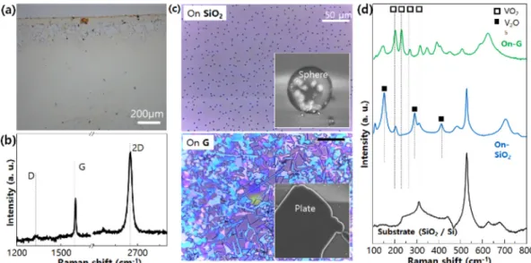
A hydrogen sensor was fabricated by utilizing a bundle of metal oxide nanostructures whose growth positions were selectively con- trolled by utilizing graphene, which is a carbon of atomic-unit thickness. To verify the reducing ability of graphene, it was confirmed that the multi-composition metal oxide V

2

O

5

was converted into VO

2

on the graphene surface. Because of the role of graphene as a reducing catalyst, it was confirmed that ZnO and MoO
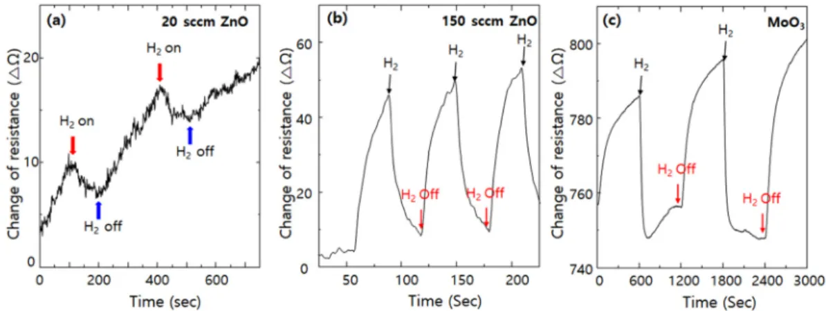
3

nanostructures were grown at high density only on the graphene surface. The fabricated gas sensor showed excellent sensitivity.

Keywords: Metal oxide, Position selective growth, Atomic carbon layer, Hydrogen sensors

1. INTRODUCTION

The increased social/public interest in hydrogen as a future energy source has led to increasing demands for its safe use [1].

When hydrogen reaches a concentration of ≥4% in the atmosphere, it reacts with oxygen and explodes; hence, the accurate monitoring of gaseous hydrogen in real time is very important. An optical-based sensor is mainly required for concentrations ≥4%, whereas at low ppb-level concentrations, an electronic sensor capable of detecting trace amounts is used [2,3].

In other words, the overall management of hydrogen concentration requires the simultaneous use of two types of sensors.

To detect very low concentrations of hydrogen, numerous studies have been conducted on an electronic sensor that utilizes the change in the resistance of a metal oxide (MO

x

) semiconductor. Hydrogen removes the OH group adsorbed on the metal oxide and increases the electron concentration on the surface, which increases the electrical conductivity of n-type oxide semiconductors; the opposite is true for p-type semiconductors [4]. To increase the sensitivity of such a gas sensor, it is necessary to increase the surface area. Thus, research has been conducted to

fabricate various metal oxide nanostructures for application in hydrogen sensors [5-8]. In general, for a nanostructured hydrogen sensor, a unit device is fabricated by forming an electrode after separating the synthesized nanostructure. If the detection device is fabricated using a single nanorod, the complex fabrication process (such as e-beam lithography) leads to lower productivity and higher processing costs. An alternative method is to synthesize a bundle of connected nanostructures to form an electrode, and then fabricating the sensor with high sensitivity.

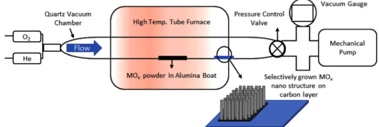
To apply such a bundle of nanostructures to a sensor, it is very important to have technology that can selectively grow nanostructures in a desired area. In this study, an atomic-unit-thick carbon layer (graphene) was used as a catalyst to control the growth position of these nanostructures. Carbon is a material with high reducing power, and the synthesis of nanostructures can be controlled by the following positional growth mechanism. The simplified chemical reaction formula is as follows:

C

(

Carbon

)

+ MO x (Powder) → CO

2(

gas

)

+ Metal

(

gas

)

Metal

(

gas

)

+ O

2(

gas

)

→ MO x

(

nanostructure

)

(on graphene)

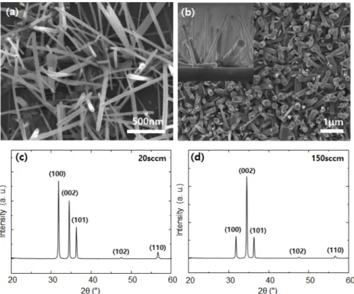
To realize this idea experimentally, we focused on ZnO (n-type, T melt = 1975

o

C) and MoO

3

(n-type, T melt = 795

o

C) catalysts. The MO

x

nanostructures, which are automatically connected to each other owing to high-density nucleation on the graphene layer, are directly applied as gas sensors, specifically for hydrogen molecules.

1

Department of Materials Science and Engineering & Department of Energy Systems Research, Ajou University, Suwon, 16499, Republic of Korea

+

Corresponding author: [email protected]

(Received: Nov. 24, 2020, Revised: Nov. 28, 2020, Accepted: Nov. 29, 2020)

This is an Open Access article distributed under the terms of the Creative Commons Attribution Non-Commercial License(https://creativecommons.org/

licenses/by-nc/3.0/) which permits unrestricted non-commercial use, distribution,

and reproduction in any medium, provided the original work is properly cited.

(2)

no. 248614, ACS reagent, 98.0%) for 1 min. Then, it was rinsed with deionized water. The etched Cu foil was loaded into a quartz tube with a base pressure of ~10

-3

Torr. Heat treatment was conducted at 1000

o

C (heating speed: 16.67

o

C/min) with a H

2

gas flow of 40 sccm. CH

4

gas was introduced into the tube at 10 sccm for 10 min. The tube was rapidly cooled to room temperature to precipitate the graphene on the catalyst surface under a H

2

gas flow of 40 sccm.

2.2 Metal oxide growth

Two different MO

x

powder sources were used for carbothermal transport: ZnO (Sigma-Aldrich, item No. 96479) and MoO

3

(Sigma-Aldrich, item No. M0753). The MO

x

powder was mixed with graphite powder (99%, Daejung, item No. 4071-1400) at an atomic ratio of 1:2, and placed at the center of quartz tubes with alumina boats. The substrates (half of the SiO

2

surface was covered with graphene) were placed at the end of a furnace 15 cm away from the boat (see Fig. 1). The vacuum pressure was reduced to 5 mTorr using a mechanical pump. Helium gas (He) was introduced into the tube at a flow rate of 40 sccm while heating for 1 h until the growth temperature was reached. The alumina boats with the source materials were heated at the center of the furnace to 900−1000

o

C (ZnO) and 600

o

C (MoO

3

). After

a He-Ne excitation source (532 nm), with a laser beam spot size of 1 µm in diameter, and an accumulation time of 60 s. X-ray diffraction was performed with a Rigaku MiniFlex spectrometer (XRD; 3 kW, Cu-Kα, HD307172) at a scan speed of 2

o

/min.

Scanning electron microscopy (SEM) images were acquired.

Hydrogen gas sensing tests were conducted using a Keithley-4200 instrument in a vacuum probe station chamber at room temperature for ZnO, and at 200

o

C for MoO

3

. Owing to the high density of MO

x

nanostructures, direct electrical wiring on the MO

x

surface was done by silver paste (ELCOAT P-100, CANS) without an additional process. The distance between the electrodes was 0.5 cm.

3. RESULTS AND DISCUSSIONS

To verify the reducing power of graphene, a CVD deposition experiment was conducted using V

2

O

5

powder of the V-O system.

The synthesized graphene was transferred to a SiO

2

substrate (Fig.

2a) and Raman spectral analysis was performed. It can be seen that one layer of graphene was synthesized at a G/2D ratio (Fig.

2b). Then, 0.8 g of V

2

O

5

powder was loaded in the cleaned alumina boat, and the substrate was placed in reverse on the alumina boat. The alumina boat with V

2

O

5

powder was loaded in

Fig. 1. Schematic image of graphene synthesized by CVD and MO

x

growth.

(3)

a quartz tube with a base pressure of ~10

-3

Torr. Heat treatment was conducted at 700

o

C (heating speed of 17.5

o

C/min) with a He gas flow of 250 sccm.

Depending on the presence or absence of a graphene layer, the image after synthesis on an optical microscope varied (Fig. 2c).

Spherical particles formed on the SiO

2

surface without graphene, while plate-shaped structures formed in the region to which

graphene was transferred. Raman spectral analysis (Fig. 2d) confirmed that the spherical particles were V

2

O

5

, and the plate- shaped structure was VO

2

. Through this, the reducing power of the graphene layer can be verified [10].

2V

2

O

5

+ C → 4VO

2

+ CO

2

(g) ΔH = −163.9 kJ/mol

Fig. 2. (a) Digital camera image of graphene transferred on Si substrate. (b) Raman spectra of each layer of graphene. (c) OM and SEM images of vanadium oxides grown on SiO

2

and graphene. (d) Raman spectra of various shapes (sphere on SiO

2

and plane on graphene) of vana- dium oxides.

Fig. 3. (a) Time vs. temperature graph for the MO

x

nanostructure growth. SEM images of MO

x

grown on half of SiO

2

/Si(100) substrates cov-

ered by transferred graphene: (b) ZnO grown at 970 °C; and (c) MoO

3

grown at 600

o

C. XRD patterns of MO

x

nanostructures grown

on graphene/SiO

2

/Si (100): (d) ZnO and (e) MoO

3

.

(4)

the MO

x

nanostructures was confirmed by XRD. The XRD profile of wurtzite ZnO (Fig. 3d) shows that it predominantly adopts the (002) preferred orientation because the hexagonal structure of graphene can act as a buffer layer and reduce the lattice mismatch.

MoO

3

(orthorhombic crystal structure, a = 3.9628 Å, b = 13.855 Å, and c = 3.6964 Å) was grown on graphene with partially vertical and rectangular nanodisk shapes (Fig. 3e) because of the relatively long lattice constant of b, resulting in a high-order diffraction profile with (020), (040), and (060) peaks. The vertically connected nanodisk MoO

3

with high density may have a large surface-to-volume ratio and exhibit higher surface sensitivity than bulk films.

To confirm the effects of changing the arrangement and shape

surface and the side wall of the pre-grown ZnO with random orientation (Fig. 4c). At a high oxygen flow rate (150 sccm), the vapor–solid growth mechanism was dominant because the Zn atoms that evaporated during the carbothermal reaction quickly reacted with sufficient oxygen, and a high flux of ZnO vapor was solidified on graphene with a (002) preferred orientation (Fig. 4d).

High-density MO

x

nanostructures with a large surface-to-volume ratio can be applied in hydrogen gas sensors. Fig. 5 shows the change in the resistance of the gas sensors fabricated using the MO

x

nanostructures (ZnO and MoO

3

) with respect to the on/off switching of 10% hydrogen gas diluted with nitrogen gas at a fixed DC voltage of 1 V. The ZnO- and MoO

3

-based sensors showed fast on/off switching characteristics resulting from typical

Fig. 4. (a, c) SEM images and XRD patterns of ZnO nanostructures grown at 1000

o

C under 20 sccm oxygen flow rate. (b, d) Top-view and

cross-sectional (inset) SEM images and XRD patterns of ZnO nanorods grown at 1000

o

C under 150 sccm oxygen flow rate.

(5)

n-type surface semiconductor gas sensors. Specifically, in the case of ZnO, depending on the growth conditions, the injection of 150 sccm of oxygen yielded better sensor characteristics compared with the injection of 20 sccm of oxygen. This is attributed to insufficient oxidation and the increase in the ratio of metallic Zn to ZnO.

4. CONCLUSIONS

In summary, the thermal transport growth of various MO

x

nanostructures using graphene as a catalytic layer was studied.

The sp

2

-bonded carbon atoms of graphene readily formed metal- carbide bonds, resulting in the preferred nucleation of MO

x

on the transferred graphene area. By using this experimental protocol, the position of the MO

x

nanostructures as well as the growth parameters, such as nucleation density and growth rate, were controlled. The position-selective and density-controlled MO

x

nanostructures were evaluated for hydrogen gas sensors. The ZnO and MoO

3

nanostructures exhibited the typical behavior of n-type semiconductor gas sensors with stable sensitivity. We believe that the graphene catalytic layer can be applied in various fields and devices that employ the growth of functional MO

x

nanostructures.

ACKNOWLEDGMENT

This research was supported by the Basic Science Research Program through the National Research Foundation of Korea (NRF), funded by the Ministry of Science, ICT & Future Planning (NRF-2019R1A2C1006972).

REFERENCES

[1] K. J. Choi and H. W. Jang, “One-Dimensional Oxide Nano- structures as Gas-Sensing Materials: Review and Issues”, Sensors, Vol. 10, pp.4083-4099, 2010.

[2] Z. Zhao, M. A. Carpenter, H. Xia, and D. Welch, “All-opti- cal hydrogen sensor based on a high alloy content pal- ladium thin film”, Sens. Actuator B, Vol. 113, pp.532-538, 2006.

[3] X. H. Chen and M. Moskovits, “Observing catalysis through the agency of the participating electrons: Surface-chemistry- induced current changes in a tin oxide nanowire decorated with silver”, Nano Lett., Vol. 7, pp.807-812, 2007.

[4] H. T. Wang, B. S. Kang, F. Ren, L. C. Tien, P. W. Sadik, D.

P. Norton, S. J. Pearton, and J. S. Lin, “Hydrogen-selective sensing at room temperature with ZnO nanorods”, Appl.

Phys. Lett., Vol. 86, pp.243503(1)-243503(3), 2005.

[5] U. T. Nakate, R. Ahmad, P. Patil, Y. T. Yu, and Y. B. Hahn,

“Ultra thin NiO nanosheets for high performance hydrogen gas sensor device”, Appl. Surf. Sci., Vol. 506, pp.144971(1)- 144971(8), 2020.

[6] Y. Wang, B. Liu, D. Cai, H. Li, Y. Liu, D. Wang, L. Wang, Q. Li, and T. Wang, “Room-temperature hydrogen sensor based on grain-boundary controlled Pt decorated In

2

O

3

nanocubes”, Sens. Actuator B, Vol. 201, pp.351-359, 2014.

[7] S. Aygün and D. Cann, “Hydrogen sensitivity of doped CuO/ZnO heterocontact sensors”, Sens. Actuator B, Vol.

106, pp.837-842, 2005.

[8] X. Hu, J. C. Yu, J. Gong, Q. Li, and G. Li, “α-Fe

2

O

3

Nanor- ings Prepared by a Microwave-Assisted Hydrothermal Pro- cess and Their Sensing Properties”, Adv. Mater., Vol. 19, pp.2324-2329, 2007.

[9] H. K. Yu, “Effective reduction of copper surface for clean graphene growth”, J. Electrochem. Soc., Vol. 162, pp. E277- E281, 2015.

[10] H. J. Lee, U. J. Yang, K. N. Kim, S. Park, K. H. Kil, J. S.

Kim, A. M. Wodtke, W. J. Choi, M. H. Kim, and J. M Baik,

“Directional Ostwald ripening for producing aligned arrays of nanowires”, Nano Lett., Vol. 19, pp.4306-4313, 2019.

Fig. 5. H

2

(10% diluted with nitrogen gas) sensing tests (a, b) employing ZnO at room temperature, and (c) MoO

3

at 200

o

C.

수치

Fig. 1. Schematic image of graphene synthesized by CVD and MO x  growth.
Fig. 2. (a) Digital camera image of graphene transferred on Si substrate. (b) Raman spectra of each layer of graphene
Fig. 4. (a, c) SEM images and XRD patterns of ZnO nanostructures grown at 1000 o C under 20 sccm oxygen flow rate
Fig. 5. H 2  (10% diluted with nitrogen gas) sensing tests (a, b) employing ZnO at room temperature, and (c) MoO 3  at 200 o C

참조

관련 문서

The limit is therefore the carbon char as a carrier utilizing only 27% of available hydrogen but sequestering 91kg of carbon dioxide (as measured experimentally) per million

ƒ The shearing process involves cutting sheet metal by subjecting cutting sheet metal by subjecting it to shear stresses, usually between a punch and a die.. ƒ

 Casting is a manufacturing process by which a molten material such as metal or plastic is introduced into a mold made of sand or metal, allowed to solidify within the mold,

ƒ Reduction (환원) : reduction of metal oxides using gases such as.. ƒ Reduction (환원) : reduction of metal oxides using gases such as hydrogen

J., “Hydrogen production from partial oxidation of dimethyl ether using corona discharge plasma”, International Journal of Hydrogen Energy , Vol.. Liu C.,

Improvement of the Performance and Stability of Oxide Semiconductor Thin-Film Transistors Using Double-Stacked Active Layers.. Metal oxide semiconductor

Among the various methods, plasma electrolytic oxidation (PEO) is a method for surface processing in which a biocompatible oxide film is formed using a number of ions..

“Act of Low Carbon Green Growth (bill)” defines a term of the ‘green growth’ as “harmony out of economic growth and the environment” which reduce climate