ISSN 1225-7591(Print) / ISSN 2287-8173(Online)
Investigation of Spark Plasma Sintering Temperature on Microstructure and Thermoelectric Properties of p-type Bi-Sb-Te alloys
Jin-Koo Han, Dong-won Shin, Babu Madavali, and Soon-Jik Hong*
Division of Advanced Materials Engineering & Institute for Rare Metals, Kongju National University, Cheonan 31080, Republic of Korea
(Received March 31, 2017; Revised April 20, 2017; Accepted April 21, 2017)
···
Abstract In this work, p-type Bi−Sb−Te alloys powders are prepared using gas atomization, a mass production powder preparation method involving rapid solidification. To study the effect of the sintering temperature on the microstructure and thermoelectric properties, gas-atomized powders are consolidated at different temperatures (623, 703, and 743 K) using spark plasma sintering. The crystal structures of the gas-atomized powders and sintered bulks are identified using an X-ray diffraction technique. Texture analysis by electron backscatter diffraction reveals that the grains are randomly oriented in the entire matrix, and no preferred orientation in any unique direction is observed. The hardness values decrease with increasing sintering temperature owing to a decrease in grain size. The conductivity increases gradually with increasing sintering temperature, whereas the Seebeck coefficient decreases owing to increases in the carrier mobility with grain size. The lowest thermal conductivityis obtained for the bulk sintered at a low temperature (603 K), mainly because of its fine-grained microstructure. A peak ZT of 1.06 is achieved for the sample sintered at 703 K owing to its moderate electrical conductivity and sustainable thermal conductivity.
Keywords: Bi0.5Sb1.5Te3 alloys, Gas atomization, Spark plasma sintering, Thermoelectric properties
···
1. Introduction
Thermoelectric conversion is an emerging technology which has a capable of converting waste heat energy to electric energy (power generation), and electricity into cooling (refrigeration). The conversion efficiency is defined by a dimensionless constant called figure of merit, ZT = (α2σ/κ)T, where α is the Seebeck coefficient, σ is the electrical conductivity, κ is the thermal conductivity, and T is the absolute temperature respectively [1, 2]. In the past decades, there were several thermoelectric (TE) materials have been introduced to achieve high ZT.
Among them, bismuth-antimony-tellurium (Bi-Sb-Te) based alloys exhibit best thermoelectric properties at room temperature (300K) [3-5]. Since the discovery of thermoelectricity, the convensional single crystal process- ing methods including zone melting [6] and Bridgman [7] methods are promising and popular for manufactur-
ing TE materials. Despite their excellent thermoelectric properties, they have numerous disadvantages such as low mechanical properties due to ease of cleavage along their basal planes, and has a high-energy consumption &
low productivity [8]. To overcome these disadvantages, various researchers have been progressing to improve the characteristics of thermoelectric and mechanical proper- ties by preparing a powder using the powder metallurgi- cal processes followed by a various vacuum sintering technologies [9-11]. Gas atomization is an effective large- scale method of producing thermoelectric powders by a high pressure inert gas [12]. Since the solidification of the alloy is performed for a short time, a homogeneous and uniform microstructure with a uniform chemical composition and particle size can be produced. The con- solidation of thermoelectric powders is a crucial part in which the microstructural changes with densification could significantly affect their transport and thermoelec-
*Corresponding Author: Soon-Jik Hong, TEL: +82-41-521-9387, FAX: +82-41-568-5776, E-mail: [email protected]
tric properties. There are listed few of well sintering meth- ods such as hot pressing (HP) [13], hot extrusion (HE) [11], spark plasma sintering (SPS) [12, 14], and hot deformation (HD) [15]. Among them, the spark plasma sintering is an excellent method of producing a sintered body having a high density by performing sintering at short duration. The grain growth could eminently control during the SPS since it is rapid sintering process, which can effectively improve mechanical properties due to grain boundary hardening. In addition, the anisotropy in thermoelectric materials can neglect in SPS process in which the sintering body having uniform physical and electrical properties [12]. It is known that the microstruc- ture plays crucial role to improve thermoelectric proper- ties, thus it is necessary to control the microstructure.
Recently Wan-Ting et al argued that the SPS sintering temperature can eminently affects the Sb2-xInxTe based thermoelectric properties, in which the highest σ/K is essential to achieve higher ZT values at moderate sinter- ing conditions [16]. Thus, optimization of sintering tem- perature is one of the primary thing in consolidation process to achieve adequate microstructure with improved thermoelectric properties.
In this study, p-type Bi-Sb-Te thermoelectric powders with excess Te were prepared by gas atomization. Subse- quently, the gas atomization powders are consolidated by SPS process at a different sintering temperatures. The microstructures, and thermoelectric properties are system- atically investigated as a function of sintering tempera- ture.
2. Experimental procedure
To make the stoichiometric Bi0.5Sb1.5Te3 excess Te composition, we have taken Bi, Sb and Te granules with high purity (99.999%), purchased from Alfa acer, and thermoelectric powders were prepared by the gas atomi- zation method [12]. The gas atomized powders were mechanically sieved under 200μm for the present work.
The selected powders consolidated using spark plasma sintering with a graphite mold with an inner diameter of 25 mm. The powder was sintered at different sintering temperatures such as 663K, 703K, and 743K with main- taining co-axial pressure of 50 MPa for 10 min.
The density of the sintered body was measured using
Archimedes' method. Micro Vickers hardness tester was used for hardness. The phase of the sintered bulks were analyzed with X-ray diffraction (MiniFlex 600, Rigaku).
The fracture surface was characterized by scanning elec- tron microscopy (MIRA LMH, TESCAN). Moreover, electron backscatter diffraction (JSM-7000F, JEOL) was used to observe the grain distribution and orientation of the grains in sintered bulk. The electrical conductivity and seebeck coefficient of the thermoelectric materials were measured by thermopower measurement system (TEP-1000, Seepel) at 300~400K temperature range.
Power factor was calculated using measured electrical conductivity and seebeck coefficient. The carrier concen- tration and mobility values were measured using a Hall effect (HMS-3000, Ecopia). The thermal conductivity was measured by the thermal diffusivity (LFA-457, NETZSCH) and the specific heat. Figure of merit (ZT) was calculated using electric conductivity, the seebeck coefficient and the thermal conductivity.
3. Results and Discussion
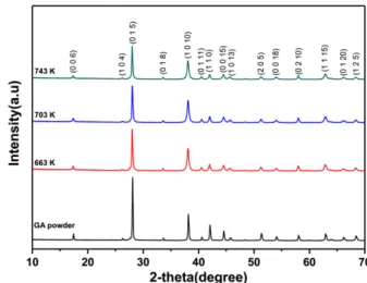
The phase of the initial gas atomized powders, and sin- tered samples (at different temperatures) were characterized by X- ray diffraction (XRD), and pattern were shown in Fig.
1. The diffraction pattern could be indexed to the Bi0.5Sb1.5 Te3 phase with a rhombohedral structure (JCPDS #49-1713), indicating that all samples were in single phase, and no
Fig. 1. X-ray diffraction patterns of Bi0.5Sb1.5Te3 thermoelectric powder by gas atomization and SPS sintered bulks at different sintering temperatures.
impurity phases were observed. Besides, the orientation factor was calculated as 0.015, 0.008, and 0.006 for sam- ples sintered at 663K, 703K, and 743K respectively. This results indicating that the orientation was very small (no preferred orientation in any special direction), and can be negligible. The relative densities were measured and obtained over 99.5% of its relative density. As pre- scribed earlier that the spark plasma sintering technique was a rapid consolidation with full densification tech- nique. The Vickers hardness was measured using hard- ness tester and shown in Table 1. The maximum hardness of 72.7Hv was obtained for sample sintered at 663K.
Since grain growth behavior, the hardness values were decreased with increase in sintering temperature. How- ever, the obtained hardness values were higher than those single crystal grown methods [17].
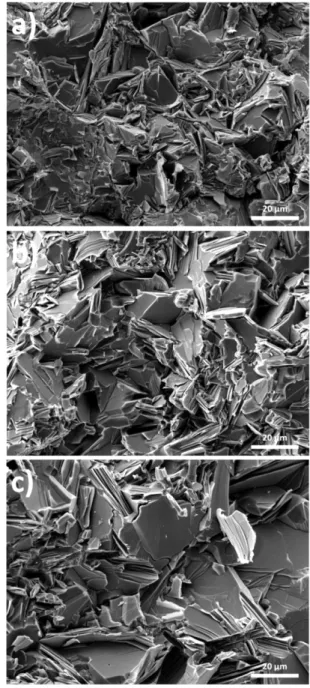
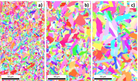
In order to analyze the bulk microstructure, grain distri- bution, and texture in bulks; the bulk fracture surfaces and EBSD texture analysis were treated. Fig. 2 shows the scanning electron micrographs of fractured surfaces of a p-type Bi0.5Sb1.5Te3 bulks sintered at (a) 663K, (b)703K, and (c) 743K respectively. It was observed that the grains are randomly distributed on the matrix, with combina- tion of submicron-order, and micron order range. This kind of bi-modal distribution of grains were from the fine and large sized gas atomized powders (few micrometers range to below 200μm), as reported in our earlier reports [12]. The bimodal microstructures can favor for increase in Seebeck coefficient, and reduction in thermal conductiv- ity, extensively due to the scattering of carriers taking places at grain boundaries in complex bimodal micro- structures. In addition, many of grains were exhibited laminar structured along the c-axis regardless of sinter- ing temperatures, which was resulted from the inherent crystal behavior of Bi2Te3-based alloys [8]. Further, tex- ture analysis was analyzed through EBSD, and shown in Fig. 3. As prescribed in the earlier, the grain size was intentionally increased as increasing sintering tempera-
tures from 663K to 743K as shown in Fig. 3(a)-(c). Each colored region/domain was representing an individual grain, and texture orientation in unique direction. It revealed that the texture was randomly orientated in entire matrix, and no such kind of preferred orientation in any unique direction was observed. This was a good agreement with the XRD pattern analysis in which no basal plane intensities were orientated. The increase in Table 1. Relative density and Vickers hardness of Bi0.5Sb1.5Te3
samples sintered at 663K, 703, and 743K respectively Relative density (%) Vickers Hardness (Hv)
663K 99.56 72.71
703K 99.46 67.41
743K 99.56 63.15
Fig. 2. SEM Fractured surfaces of Bi0.5Sb1.5Te3 bulks fabricated by SPS at a) 663K, b) 703K, and c) 743K temperatures. The fracture surface represents bi-model microstructure of bulk samples regardless of sintering temperatures.
grain size could severely affected the transport properties in thermoelectric materials. It was known that the large grains can induce the high carriers transport from one to another, as compared with fine grains. Such kind of car- rier transportation behavior can increase the carrier mobility in matrix, which benefits to increases in electri- cal conductivity.
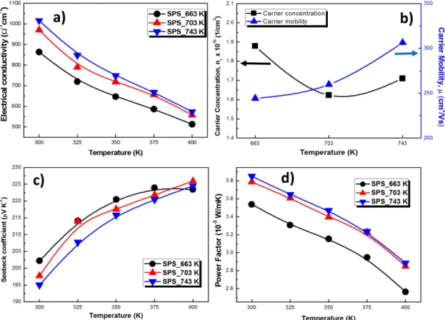
The temperature dependence of the thermoelectric properties of p-type Bi0.5Sb1.5Te3 samples with different temperatures were shown in Fig. 4. All measurements were carried out along the direction perpendicular to the SPS pressing direction. The electrical conductivity (shown in Fig. 4(a)) decreased with temperature for all samples, exhibiting a degenerate semiconductor behavior. The electrical conductivity increased gradually with increase in sintering temperature and can be attributed to the increases in carrier mobility (μ), as shown in Fig. 4(b).
The peak electrical conductivity of 1016Ω-1cm-1 was obtained for the SPS-743K sample at RT. In general, the electrical conductivity (σ) can be expressed as [12]
σ = neµ (1)
where n is the carrier concentration, and e is the carrier charge. The measured n, and µ were shown in Fig. 4(b).
The carrier mobility increased with increasing sintering
temperature from 663K to 743K, which was attributed to the increase in grain size. Besides, the carrier concentra- tion was slightly decreased with sintering temperature.
However, the magnitude of the increase in mobility was high, which was caused to increase in electrical conduc- tivity with sintering temperatures.
The temperature dependent Seebeck coefficients (α) of Bi0.5Sb1.5Te3 samples with different temperatures were shown in Fig. 4 (c). All sintered samples show positive Seebeck coefficient values indicating a p-type semicon- ducting behavior. The Seebeck coefficient values of 202, 197, and 195μV/K obtained for the samples sintered at 663K, 703K, and 743 K at RT respectively. It was noticed that the α values decreased with increase in sin- tering temperature mainly due to the increase in carrier mobility.
It is known that the Seebeck coefficient (α) of p-type Bi0.5Sb1.5Te3 materials were severely influenced by the carrier mobility, can be represented as follows [4, 12]
(2)
where kB is the Boltzmann’s constant, h is the Plank’s con- stant, τ is the relaxation time [(eτ/µ) = m*]. The increase in carrier mobility should be severely affected the Seebeck coefficient, as from the expression (2), thus finally
α 8π2kB2T 3qh2 --- eτ
--- πμ 3n ---
⎝ ⎠⎛ ⎞2 3⁄
=
Fig. 3. Texture analysis of Bi0.5Sb1.5Te3 bulks fabricated by SPS at a) 663K, b) 703K, and c) 743K temperatures. The texture analysis indicating no preferred orientation in any direction.
decreased its values with increase in sintering tempera- ture. The power factor, PF can be calculated from the square of the Seebeck coefficient with electrical conduc- tivity was shown in Fig. 4(d). The power factor values decreased with increase in measurement temperature as like electrical conductivity. The peak PF of 3.85 W/mK2 was obtained at RT for SPS-743K sample, and decreased its value with decrease in sintering temperatures. The increase in electrical conductivity could be more contrib- uted to the increase in power factor for the samples with sintering temperatures.
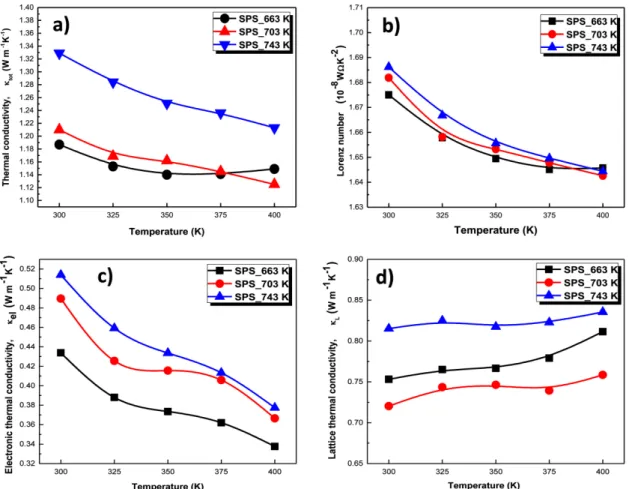
Fig. 5 shows the thermal transport properties of p-type Bi0.5Sb1.5Te3 samples at different temperatures. The total thermal conductivity κtot is the sum of electronic compo- nent κe, and the lattice component κL. The electronic ther- mal conductivity can be calculated by the Widemann- Franz Law; κe=σLT, where L is the Lorentz number, σ is the electrical conductivity, T is the absolute temperature, respectively [18]. The total thermal conductivity was shown in Fig. 5(a), and noticed that κtot was minimum for
low sintering temperatures, and increased as increase in sintering temperatures. In order to calculate that electronic component of thermal conductivity, Lorentz number should be determined. The Lorentz number is estimated from the single parabolic model, and plotted in Fig. 5(b).
The estimated Lorentz values were lower than the degener- ate semiconductor materials (L=2.45×10⁻⁸ WΩK-2) [19].
The electronic components of thermal conductivity (κe) can be calculated by using estimated Lorentz numbers, and drawn in Fig. 5(c). The κe values decreased with increase in sintering temperature, which is proportional to the electrical conductivity. Further, the lattice thermal con- ductivity, (κL) (shown in Fig. 5(d)) was low at low sinter- ing temperatures, suggesting that fine grains were inhibit the phonon propagation in matrix. Finally, the obtained low κtot are mainly attributed to the fine grain microstruc- ture at low sintering conditions, in which the carriers/
phonons can eminently blocked at fine grain boundaries [10]. The reduction thermal conductivity could benefit for the enhancement of figure of merit, discussed in the Fig. 4. Temperature dependence of (a) electrical conductivity, (b) carrier concentration, and mobility, (c) Seebeck coefficient, and (d) Power Factor of Bi0.5Sb1.5Te3 bulks fabricated by SPS at different temperatures.
following section.
The temperature dependence of the figure of merit, ZT was shown in Fig. 6. It was evident that the sample sin-
tered at 703K shows high ZT values than other samples.
The peak ZT of 1.06 was achieved for the SPS-703K sample at 375K. It should be noted that the SPS-703K sample exhibit moderate electrical conductivity with sus- tainable thermal conductivity values, this could cause to increase in Figure of merit. The improved large-scale production of p-type Bi0.5Sb1.5Te3 samples by gas atomi- zation and SPS can beneficial for commercialization of thermoelectric applications.
4. Conclusion
P-type Bi-Sb-Te alloys powders were successfully pro- duced by gas atomization process, and consequently con- solidated with spark plasma sintering (SPS) at 603K, 703K, and 743K. The phase structure of both powders and sintered bulks were analyzed by X-ray diffraction.
The severe grain growth behavior was observed with Fig. 5.Temperature dependence of (a) Total thermal conductivity, (b) Lorentz number, (c) electronic thermal conductivity and (d) Lattice thermal conductivity of Bi0.5Sb1.5Te3 bulks fabricated by SPS at different temperatures.
Fig. 6. Temperature dependence of figure of merit of Bi0.5Sb1.5 Te3 bulks fabricated by SPS at different temperatures.
increase in SPS sintering temperature, which would mainly influence the mechanical, and thermoelectric transport properties. The hardness was gradually decreased with sin- tering temperature, which was mainly attributed to the grain growth behavior. The electron back scattering dif- fraction analysis revealed that the grains were randomly orientated in entire matrix, and no grains were preferably orientation in any unique direction. The temperature dependence of electrical conductivity increased with sinter- ing temperature, while the Seebeck coefficient decreased slightly due to the increases in carrier mobility with grain size. The maximum ZT of 1.06 was achieved for the sample sintered at 703K due to exhibiting their favorable electrical conductivity and thermal conductivity values.
Acknowledgement
This work was supported by the Korea Institute of Energy Technology Evaluation and Planning (KETEP) granted financial resource from the Ministry of Trade, Indus- try & Energy, Republic of Korea (No.20152020001210).
References
[1] M. S. Dresselhaus, G. Chen, M.Y. Tang, R. Yang, H. Lee, D. Z. Wang, Z. F. Ren, J. P. Fleurial and P. Gogna: Adv.
Mater., 19 (2007) 1043.
[2] K. F. Hsu, S. Loo, F. Guo, W. Chen, J. S. Dyck, C. Uher, T. Hogan, E. K. Polychroniadis and M. G. Kanatzidis:
Science, 303 (2004) 818.
[3] B. Poudel, Q. Hao, Y. Ma, Y. Lan, A. Minnich, B. Yu, X.
Yan, D. Wang, A. Muto, D. Vashaee, X. Chen, J. Liu, M.
S. Dresselhaus, G. Chen and Z. Ren: Science, 320 (2008)
634.
[4] J. H. Son, M. W. Oh, B. S. Kim, S. D. Park, B. K. Min, M. H. Kim and H. W. Lee: J. Alloys Compd., 566 (2013) 168.
[5] P. Rimal, S. M. Yoon, E. B. Kim, C. H. Lee, S. J. Hong:
J. Korean Powder Metall. Inst., 23 (2016) 2.
[6] D. Liu, J. Stotzel, M. Seyring, M. Drue, X. Li, R.
Schmeche and M. Rettenmayr: Cryst. Growth Des., 16 (2016) 617.
[7] O. Yamashita and H. Odahara: J. Mater. Sci., 41 (2006) 323.
[8] X. Tang, W. Xie, H. Li, W. Zhao, Q. Zhang and M. Niino:
Appl. Phys. Lett., 90 (2007) 012102.
[9] Y. Lan, B. Poudel, Y. Ma, D. Wang, M. S. Dresselhaus, G.
Chen and Z. Ren: Nano Lett., 9 (2009) 1419.
[10] W. Xie, J. He, H. J. Kang, X. Tang, S. Zhu, M. Laver, S.
Wang, J. R. D. Copley, C. M. Brown, Q. Zhang and T. M.
Tritt: Nano Lett., 10 (2010) 3283.
[11] S. J. Hong, Y. S. Lee, J. W. Byeon and B.S. Chun: J.
Alloys Compd., 414 (2006) 146.
[12] B. Madavali, H. S. Kim, K. H. Lee, Y. Isoda, F. Gascoin and S. J. Hong: Mater Des., 112 (2016) 485.
[13] K. F. Cai, C. W. Nan, M. Schmuecker and E. Mueller: J.
Alloys Compd., 350 (2003) 313.
[14] M. L. Lwin, S. Yoon, B. Madavali, C. H. Lee, S. J. Hong:
J. Korean Powder Metall. Inst., 23 (2016) 120.
[15] L. P. Hu, H. Gao, X. Liu, H. Xie, J. Shen, T. Zhu, and X.
Zhao: J. Mater. Chem., 22 (2012) 16484.
[16] W. T. Chiu, C. L. Chen and Y. Y Chen: Sci. Rep., 6 (2016) 23143.
[17] X. A. Fan, J. Y. Yang, R. G. Chen, H. S. Yun, W. Zhu, S.
Q. Bao and X. K. Duan: J. Phys. D : Appl. Phys., 39 (2006) 740.
[18] J. Li, Q. Tan, J. F. Li, D.W. Liu, F. Li, Z. Y. Li, M. Zou and K. Wang: Adv. Funct. Mater., 23 (2013) 4317.
[19] N. Keawprak, Z. M. Sun, H. Hashimoto and M. W. Bar- soum: J. Alloys Compd., 397 (2005) 236.