I. Introduction
In recent years, the increase of data transmission over the internet has led to the demand for high-speed serial-data communication networks.
Several optical communication standards have been applied to high-speed and long-distance communications. Considerable design efforts have been focused on low-cost, low-power integrated fiber-optic transmitters and receivers. CDR can be used for receivers to generate the clocks synchronized with received data.
One of challenges which are required to design CDR is phase-frequency detectors (PFDs) dealing
3.125Gbps Reference-less Clock and Data Recovery using 4X Oversampling
4X 오버샘플링을 이용한 3.125Gbps급 기준 클록이 없는 클록 데이터 복원 회로
張 亨旭*, 姜 晉球*★
Hyung-Wook Jang* , Jin-Ku Kang*★
Abstract
In this paper, a clock and data recovery (CDR) circuit for a serial link with a half rate 4x oversampling phase and frequency detector structure without a reference clock is described. The phase detector (PD) and frequency detector (FD)are designed by 4X oversampling method. The PD, which uses bang-bang method, finds the phase error by generating four up/down signal and the FD, which uses the rotational method, finds the frequency error by generating up/down signal made by the PD output. And the six signals of the PD and the FD control an amount of current that flows through the charge pump. The VCO composed of four differential buffer stages generates eight differential clocks. Proposed circuit is designed using the 0.18um CMOS technology and operating voltage is 1.8V. With a 4X oversampling PD and FD technique, tracking range of 24% at 3.125Gbps is achieved.
요 약
본 논문에서는 기준동작 클럭없이 데이터만으로 구현되는 반주기의 4x 오버샘플링 위상/주파수검출기를 이용한 클럭 데이터 복원회로에 대하여 서술하였다. 위상 및 주파수검출기는 4x 오버샘플링 기법을 이용하여 설계되었다.
위상검출기는 뱅뱅 제어방법에 의해, 주파수검출기는 로테이션방법에 의해 동작한다. 위상 및 주파수 검출기로부 터 발생된 6개의 신호들은 전하펌프로 들어갈 전하량을 결정한다. VCO단은 4개의 차동 지연단으로 구성되고 8개 의 클럭신호를 생성한다. 제안된 회로는 공급전압 1.8V, 0.18um MOCS 공정으로 설계 시뮬레이션되었다. 제안된 구조의 PD와 FD를 사용하여 25%의 넓은 트래킹 주파수 범위를 가진다.
Key words: Clock and data recovery (CDR), frequency detector, Phase detector, 4X Oversampling
* 인하대학교 전자공학과
(Dept. of Electronics Engineering, Inha University)
★교신저자 (corresponding author)
接受日:2005年 2月 6日, 修正完了日: 2005年 12月 25日
withmissing data transitions in NRZ data format. In convention, Hogge type phase detector(PD), Alesander type PD, tri-wave type PD, or quadricorrelator structures are used for CDR circuits. A three state PFD can not be used in CDR application because the data missing causes error pulses. In other CDR architectures, the oversampling algorithm was applied. These usually adopt 1:N demultiplexing architectures for relaxing the processing speed after very high oversampling the input. This paper proposes a clock and data recovery circuit that has a half rate PD and FD using 4x-oversampling method [1] without a reference clock. The proposed circuit adopts the tracking PLL structure for phase and frequency locking. A 3.125Gbps reference-less CDR is implemented with a half-rate bang-hang phase detector and a rotational frequency detector using 4x oversampling method in this work
II. Architecture
4X- Oversampling
PD
FD
Pup1 Pdn1 Pup2
Pdn2 VCO
CP1
CP2
CP3
Clk0,Clk0b~Clk3,Clk3b Clk0,Clk0b~Clk3,Clk3b
Input data
Recovered Data
Clk2 Fup
Fdn
MUX
Dout0
Dout4
Fig. 1. Block diagram of the proposed system 그림 1.제안하는 구조의 블록도
The proposed architecture is shown in Fig.1. Input data are sampled by 8 clock signals generated at the output of a four stage differential VCO then the phase and frequency detector circuit produces phase and frequency error information with 8 sampled data. Due to the small capture range of the phase detector, a frequency detector is required to make frequency acquisition. The outputs of the phase and frequency detectors control three charge-pumps and loop filter to provide the control voltage for the VCO. And three charge pumps have individually a different amount of current. Then, the VCO which is controlled with charge pump and loop filter
generates 8 clock signals which have 45 degree difference. Finally, the MUX controlled with clk2 signal is used to produce the retimed data from Dout0 and Dout4
III. Phase detector
4X Oversampler
Transition detector (XOR)
Clk1
Clk0 Phase Up /Down
Controller (Switch)
Pup1 Pdn1 Pup2 Pdn2 Clk3
Clk2 Clk0,Clk0b~Clk3,Clk3b
MULTIPHASE
3.125 Gbps input data
Fig. 2. Block diagram of the phase detector 그림 2. 제안하는 위상검출기 블록도
The block diagram of a half-rate bang-bang phase detector is shown in Fig. 2. The phase detector uses eight clock signals (clk0,clk0b~clk3,clk3b) to detect data transition for two consecutive incoming data. Eight samplers sample eight data for two successive input data. Through eight XOR gates, these samples provide four output signals that control two charge pumps (CP1, CP2) and loop filter to generate the VCO control voltage for a phase error.
Phase lock I II III IV
Clk0 Clk1 C lk2 Clk3 Clk0b C lk1b Clk2b VII
V VI
Clk3b
Pdn1
Pup1 I II III IV
Clk0 Clk1 Clk2 Clk3 Clk0 b Clk1b Clk2b VII
V VI
C lk3b
IV III
I II
Clk0 Clk1 C lk2 Clk3 Clk0b Clk1b Clk2b VII
V VI
Clk3b Clk0
Clk0
Clk0
Pup2 I II III IV
Clk0Clk1 Clk2 Clk3 Clk0b Clk1b Clk2b VII
V VI
Clk3 b Clk0
Pdn2 I II III IV
Clk0 Clk1 Clk2 Clk3 Clk0b Clk1b Clk2b VII
V VI
C lk3b C lk0
Fig. 3. Condition of the PD up/down signal 그림 3. 위상검출기의 up/down신호 생성 조건 Fig. 3. shows the condition of PD up/down signals.
In this condition, Pup1 and Pdn1 signals are
generated in the case of a small phase error and Pup2 and Pdn2 signals are generated in the case of a large phase error.
If the PD is locked, the data transition happens on the clk2 and clk2b signal. Using four steps with 4x oversampling instead of the conventional two steps phase adjustment increases the linearity of the bang-bang phase detector and results in both low jitter generation and high lock-in range [2].
Pup1-1 Pup1-2 Pdn1-1 Pdn1-2 Pup2-1 Pup2-2 Pdn2-1 Pdn2-2
clk1 clk0 clk2 clk3
Pup1-1 Pup1-2
Pdn1-1 Pdn1-2
Pdn1-2
Pup2-1 Pup2-2 Pup2-1
Pup2-2
Pdn2-1 Pdn2-2
Pdn2-2 Pdn2-1
Pup1 signal
Pup2 signal Pdn2 signal Pdn1 signal Clock
Pup1-2 Pup1-1
Fig. 4. Timing diagram of the PD up/down signal 그림4. 위상검출기 up/down 신호의 타이밍도 Fig 4. shows the timing diagram of the four PD up/down signals. A data transition between clk1 and clk2 causes Pup1-1 signal to generate and adata transition between clk1b and clk2b causes Pup1-2 signal to generate. Then Pup1-1 and Pup1-2 signals are switched with clk1 signal to Pup1 signal. Pdn1, Pup2, and Pdn2 signal of the PD are also generated with the same manner.
IV. Frequency detector
In this paper, FD used the rotational architecture.
Fig. 5. shows the block diagram of the frequency detector. The FD uses Pup1, Pup2, and Pdn2 signals of the PD to detect frequency error. And the FD is disenabled with Pup1 signal when the frequency of this CDR is locked.
Frequency Up /Down Controller
Fup Fdn
Pup2 Pdn2 Pup1
Fig. 5. Block diagram of the frequency detector 그림 5. 주파수 검출기의 블록도
Fig. 6. shows the condition of the FD up and down signal. Because the FD uses the rotaional method, if the consecutive data transitions occur from I to IV or from V to VII, FD generates a frequency up signal. Otherwise, if the successive data transitions occur from IV to I or from VII to V, FD generates a frequency down signal.
Frequency Up : I Frequency Down : IV
I II III IV V VI VII VIII I Clock
Fig. 6. Condition of the FD up/down signal 그림6. 주파수검출기의 up/down 신호 조건
V. Circuit design
Sampler
Sampler
Sampler
Sampler
Sampler
Sampler
Sampler
Sampler Clk0
Clk1
Clk2
Clk3
Clk0b
Clk1b
Clk2b
Clk3b
Data
Dout0 Dout1
Dout2
Dout3
Dout4
Dout5
Dout6
Dout7
Dout0 I
II
III
IV
V
VI
VII
VIII I V
IV VIII
II VI
III VII
Clk0
Clk1
Clk2
Clk3 Pup2
Pdn2
Pup1
Pdn1
Fig. 7. Schematic of the PD 그림. 7. 위상검출기의 회로도
Fig. 7. shows schematic of the phase detector with four up/down signals. Eight data are sampled with not a D-F/F but a sampler in the each positive edge of eight clocks (clk0,clk0b, ~clk3, clk3b). And eight XOR gates are used to detect data transitions.
Then four switches were used to generate four up/down signal which are Pup1, Pdn1, Pup2, and Pdn2. Four switches are individually controlled with clk0, clk1, clk2, and clk3 signal.
Q
SET Q
CLR
D
Q
SET Q
CLR
D
Q
SET Q
CLR
D
Pup2 Pdn2
Pup1
Fup
Fdn
Fig. 8. Schematic of the FD 그림8 주파수검출기 회로도
The delay buffer used in VCO is shown in Fig. 9.
Because the effective resistance of the load elements changes with the bias voltage, the buffer's delay varies with the bias voltage Vbp. This bias voltage is generated by the feedback network of the phase frequency detector, charge pump and loop filter.
These load elements lead to good control over delay and high dynamic supply noise rejection [4].
Fig. 9. Schematic of the Delay buffer 그림 9. 지연 버퍼의 회로도
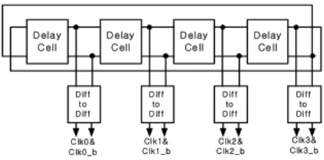
D ela y C ell
D elay C ell
D elay Ce ll
D elay Ce ll
D iff t o D iff
D iff to D iff
D iff to D iff
Di ff to Di ff
C lk0 &
C lk0_ b
Cl k1&
C lk1 _b
C lk2 &
C lk2 _b
C lk3 &
C lk 3_ b
Fig. 10. VCO and multiple-phase clock generation 그림 10. 다중위상 생성기 및 VCO 블록도
Four delay stages in the VCO are locked at 2π
-phase shift. Thus, for 1.5625Ghz application, the delay value in the VCO is set to be 80ps.Because the operating voltage swing level of the core VCO-cell is small, the full-swing circuit was added to drive the PFD circuit. The whole VCO circuit diagram is shown in Fig. 10.
VI. Simulation
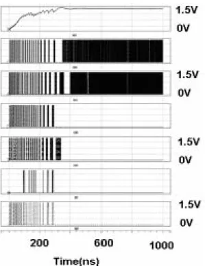
The design was simulated with TSMC 0.18um CMOS technology. The data rate of 3.125Gbps with 1.5625GHz recovered clock was original design target. The multiphase clocks used in this paper is generated from the VCO of 4 delay cells. The maximum number of consecutive input data is 4 and the initial voltage controlling the VCO is near the bias point where the clock and input data are synchronized. When CDR is locked at 3.125Gbps random input data, Fig. 11. shows CDR control signals which is required to be locked state and Fig. 12 illustrates the recovered clock, input data, and the recovered output data.Since the FD UP/DOWN signals carried through the logic operations can turn off the charge-pump of the FD when the frequency of input data are locked, the charge-pump of the FD requires no more power consumption but two charge-pumps of the PD requires continuously power consumption because the PD uses basically the bang-bang method.The simulation on the nominal case (Typical N MOS-typical P MOS) only was executed.
Simulation on the SS(Worst-Worst) and FF(Best-Best) case could not be done because of the huge data after layout extraction. The typical variation from the simulation and the real fabricated chip was less than 10%[2]
Fig. 11. CDR control signal: (a)VCO control voltage, (b)Pup1, (c)Pdn1, (d)Pup2, (e)Pdn2, (f)Fup, (g)Fdn 그림. 11 CDR 제어신호 출력 (a) VCO 제어 전압, (b)Pup1,
(c)Pdn1, (d)Pup2, (e)Pdn2, (f)Fup, (g)Fdn
Fig. 12. CDR output signal: (a)Recovered clock, (b)Random input data (c) Recovered input data 그림 12. CDR 출력 신호(a) 복원 클럭 (b) Random 입력신
호 (c )복원 데이터
Fig. 13. shows tracking range simulation. Tracking range is 24% at 3.125Gbps. This wide tracking range can be compared to the 4-5% in other
references [2,3]. The CDR has 1.8v single power supply. The power dissipation is about 140mW. The design summary is given in Table 1
(a)
(b)
Fig. 13. VCO control voltage for tracking range simulation : (a) Frequency up case (b)
Frequency down case
그림 13. Tracking 동작범위 시뮬레이션 (a)주파수 올라갈 때 (b) 주파수 내려갈 때
Table 1. Design summary 표 1. 설계 요약표
Technology CMOS 0.18um Phase Noise -110dBc/Hz
@1Mhz offset Supply 1.7 - 1.9 volt Loop BW 250 KHz Tracking
range 1.37 - 1.75GHz Chip Area 600um*400um Jitter [email protected] Power
Dissipation 140 mW
VII. Conclusion
We described a clock and data recovery circuit with a half rate 4X oversampling PD and FD without a reference clock. The CDR circuit with PD and FD technique of 4X oversamping can find the synchronization between input data and clock by performing digital logic operations and recover theconsecutive data without an additional circuit or insertion of predefined signals. Since the circuit utilizes the digital logic for PD and FD function, it has better portability to different processes.
Simulated result shows that the circuit is capable of recovering clock and data at rates of 3.125Gbps with 0.18 um CMOS technology
VIII. Acknowledgement
This work was supported by System IC-2010 project from COSAR. And Authors also thank the IDEC and IT-SOC for its hardware and software assistance for the layout and simulation.
References
[1] Hee-sop Song, Hyung-wook Jang, Sung-sop Lee, and Jin-ku Kang "A 1.25Gb/s clock recovery ciruit using half-rate 4X-Oversamplin PFD", ISOCC '04, Oct. 26, 2004
[2] M. Ramezani, C. Andre, and T. Salama, "A 10Gb/s CDR with a Half-rate Bang-Bang Phase Detector", Cir-cuits and Systems, 2003. ISCAS '03.
Proceedings of the 2003 International Symposium on ,Volume: 2 , 25-28 May, 2003
[3] Rezayee. A, and Martin, K., "A 9-16Gb/s clock and data recovery circuit with three-state phase detector and dual-path loop architecture", European Solid-State Circuits, 2003. ESSCIRC '03. Conference on , 16-18 Sept. 2003
[4] John G. Maneatis, "Low-jitter process- independent DLL and PLL Based on Self-Biased Techniques", IEEE Journal of Solid State Circuits, Nov, 1996
저 자 소 개
장형욱 (정회원)
2000년 인하대학교 전자.전기.컴퓨 터공학부 졸업
2005년 인하대학교 전자.전기컴퓨 터공학부 석사졸업.
현재 LG Phillips LCD 안양 연구 소
<주관심분야>
CMOS고속회로 설계, VLSI, Clock Data Recovery, PLL
강진구 (正會員)
1983 서울대학교 공학사.
1990 New Jersey Institute of Technology 전자공학 석사, 1996 North Carolina State University, 전자 및 컴퓨터공학 박사.
1983-1988 삼성반도체 1996-1997 미국 INTEL 선임설계연구원.
1997. 3월 - 현재 인하대학교 전자전기공학부 교수
<주관심분야>
고속 CMOS회로설계. 혼합모드 회로설계,
PLL/DLL/CDR, High speed Interface, Display IC