1. 서 론
파워 반도체 소자는 1 W 이상의 고전압, 대전류를 제어하는 스위칭 소자를 일컫는다. 파워 반도체 소자는 스위치의 온, 오프에 따라 물질적인 특성상 작은 저항 체의 역할을 하게 되고 전력손실이 발생하게 된다. 전
✉ Ey Goo Kang; [email protected]
Copyright ©2019 KIEEME. All rights reserved.
This is an Open-Access article distributed under the terms of the Creative Commons Attribution Non-Commercial License (http://creativecommons.org/licenses/by-nc/3.0) which permits unrestricted non-commercial use, distribution, and reproduction in any medium, provided the original work is properly cited.
력 반도체 소자는 이를 개선하기 위해 낮은 전력 소자 를 구현하고 높은 항복을 목표로 발전되어 왔다 [1-5].
본 논문에서는 전력손실 감소와 소자의 신뢰성을 위하 여 낮은 온-상태 전압강하(Vce-sat)와, 높은 항복전압 (breakdown voltage)을 구현하고자 single N+ emitter trench gate type IGBT (insulated gate bipolar transistor) 소자에 대하여 T-CAD를 이용하여 새로운 구조 연구를 하였다. Trench gate의 깊이(depth)와 이 온주입(implant) 후 확산공정(drive-in)에서 온도(temp) 와 시간(time)의 변화에 따른 simulation을 통해 문턱 전압, 항복전압, 온-상태 전압강하 전기적 특성에 대한 연구를 하였다.
600 V급 IGBT Single N+ Emitter Trench Gate 구조에 따른 전기적 특성
신명철1, 육진경2, 강이구1,2
1 극동대학교 에너지반도체학과
2 극동대학교 교양학과
Study on the Electrical Characteristics of 600 V Trench Gate IGBT with Single N+ Emitter
Myeong Cheol Shin
1, Jinkeoung Yuek
2, and Ey Goo Kang
1,21 Department of Energy IT Engineering, Far East University, Uem-sung 27601, Korea
2 Department of General education, Far East University, Uem-sung 27601, Korea
(Received March 22, 2019; Revised April 25, 2019; Accepted June 1, 2019)
Abstract: In this paper, a single N+ emitter trench gate-type insulated gate bipolar transistor (IGBT) device was studied using T-CAD, in order to achieve a low on-state voltage drop (Vce-sat) and high breakdown voltage, which would reduce power loss and device reliability. Using the simulation, the threshold voltage, breakdown voltage, and on-state voltage drop were studied as a function of the temperature, the length of time in the diffusion process (drive-in) after implant, and the trench gate depth. During the drive-in process, a 20℃ change in temperature from 1,000 to 1,160℃
over a 150 minute time frame resulted in a 1 to 4 V change in the threshold voltage and a 24 to 2.6 V change in the on-state voltage drop. As a result, a 0.5 um change in the trench depth of 3.5 to 7.5 um resulted in the breakdown voltage decreasing from 802 to 692 V.
Keywords: Insulated gate bipolar transistor, Trench gate, Emitter, Breakdown voltage, Power device
DOI: https://doi.org/10.4313/JKEM.2019.32.5.366
ISSN 1226-7945(Print), 2288-3258(Online)
2. 실험 방법
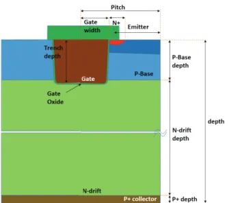
그림 1은 실험을 하기 위한 600 V급 single N+
emitter trench gate IGBT 소자의 단위 셀 구조를 나 타내고 있다.
표 1의 parameter 값은 600 V trench gate IGBT parameter를 참고한 기준으로 설정한 parameter이다 [6]. 표 1에 나와 있는 parameter를 기준으로 하여 이 온주입(implant) 후 확산공정(drive-in)에서 온도(1,000~
1,160℃) 변화와 trench gate 깊이(3.5~6.5 ㎛)를 변화 시키면서 변화에 따른 핵심적인 전기적 특성인 항복전압 (breakdown voltage)과 문턱전압(threshold voltage), 온-상태 전압강하(Vce-sat)의 변화에 대해 분석하였다.
3. 결과 및 고찰
3.1 N+ Emitter 확산 공정 온도 변화에 따른 전기적 특성
N+ 이온주입(implant) 후 확산공정(drive in) 단계 에서 150분의 동일한 시간으로 확산 온도를 1,000~
1,160℃까지 20℃씩 높이며 전기적인 특성을 분석하였다.
그림 2와 같이 확산공정에서 공정 온도가 높아질수 록 N+ 및 P–Base 영역의 접합깊이가 증가하는 것을 확인할 수 있다. Trench gate 소자의 경우 항복전압 은 trench gate의 하단에 전계집중 현상이 발생하게 된다. 그렇기 때문에 trench depth가 동일한 상태에 서 drive-in 온도를 변경시킨 이 simulation에서는 그 림 2의 (b)와 같이 오차범위 내에서 미세한 변동이 있 는 항복전압을 확인할 수 있다.
Fig. 1. Cross-sectional view of the single n+ emitter trench gate IGBT.
Table 1. Device parameters used in simulation.
Classification Unit Value
Cell pitch ㎛ 12
Cell depth ㎛ 200
Resist Ω 21
P-base dose cm2 1.7×10¹⁷
Trench depth ㎛ 8
Gate width ㎛ 4
N+ width ㎛ 1
(a)
(b)
Fig. 2. (a) P-base and n+ emitter junction depth and (b) electric field variation according to the drive-in temperature.
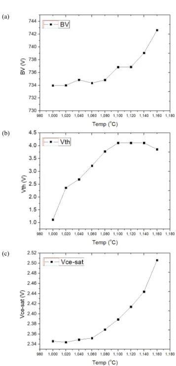
그림 3 및 표 2의 결과와 같이 확산공정 온도가 높 아질수록 P-base 영역의 접합 깊이가 증가하면서 channel 길이가 길어짐으로 인해 문턱전압은 증가하 고, 또한 channel 길이가 길어짐으로 인해 channel 저항도 증가함으로 인해 온-상태 전압강하 특성은 저 하되는 것을 확인할 수 있다.
3.2 Trench gate depth 변화에 따른 전기적 특성
그림 4와 같이 trench gate depth를 3.5~7.5 um 까지 0.5 um씩 증가시키며 etch하여 전기적 특성을 분석하였다.
그림 5는 breakdown voltage가 발생하는 순간의 전계분포도이다. 그림 5와 같이 trench gate 하단에서 부터 전계집중 현상이 발생하는 것을 확인할 수 있었 고 그림에서 보는 것과 같이 trench gate 깊이가 깊어 Table 2. The electrical characteristics of the device according to the drive-in temperature.
Temp (℃) Threshold voltage (V) Breakdown voltage (V) Vce-sat (V)
1,000 1.153 734.77 2.483
1,020 1.342 734.05 2.486
1,040 2.731 734.13 2.494
1,060 3.443 734.37 2.513
1,080 3.944 734.85 2.530
1,100 4.204 735.71 2.556
1,120 4.204 736.94 2.582
1,140 4.204 738.79 2.622
1,160 3.938 741.47 2.671
Fig. 4. The IGBT structure according to the trench gate depth.
Fig. 5. Electric field distribution according to the trench gate depth.
(a)
(b)
(c)
Fig. 3. The electrical characteristics of the device according to the drive-in temperature. (a) Breakdown-voltage, (b) threshold-voltage, and (c) on-state voltage drop.
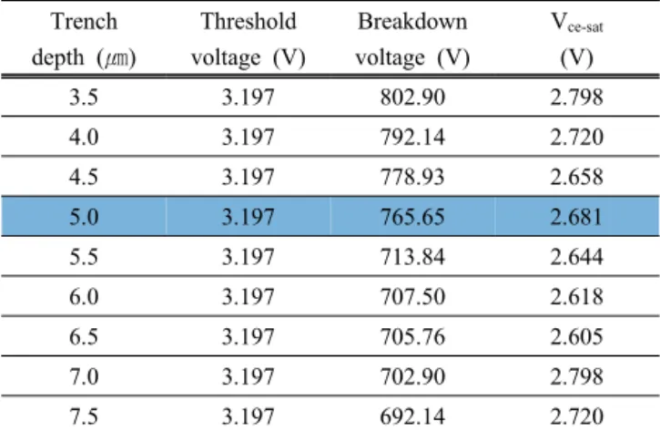
질수록 드리프트 영역이 줄어들어 항복전압 특성이 감 소하는 것을 확인할 수 있었다.
그림 5의 전계분포를 원인으로 그림 6과 같은 결과 를 확인할 수 있었다. Trench gate depth가 깊어질수
록 drift의 공핍층이 형성되는 영역이 줄어들게 되면서 항복전압 특성이 저하되고, Drift 영역만큼 저항이 줄 어들게 됨으로 인해 온-상태 전압강하 특성이 향상되 는 것을 확인할 수 있었다.
4. 결 론
본 연구 결과를 통해 N+ emitter 이온 주입 후 공정 온도는 1,100℃, trench gate depth는 5 um, 목표 항복 전압으로 600 V를 넘는 것을 확인하여 single emitter source trench IGBT에 적합한 것을 확인할 수 있다.
N+ emitter drive in 단계에서 온도를 높게 하거나 공정시간을 길게 진행할수록 항복전압, 온-상태 전압 강하가 변화하는 것을 확인하였고, 문턱전압은 큰 변화 가 없음을 확인할 수 있었다. 또한 trench depth가 깊어질수록 항복전압의 특성은 저하되고, 온-상태 전 압강하가 특성은 향상되는 트레이드오프 관계를 확인 할 수 있었다.
전계가 집중되는 것을 방지하여 온-상태 전압강하 특성을 향상시키기 위해 제시한 구조로서 연구를 진행 해 보았다. 이번에 연구해 보고자 했던 목적은 FDT IGBT의 구조에서 dummy trench gate가 없을 때에도 Vce-sat의 특성 향상을 연구해 보고자 했지만 simulation 결과 Vce-sat 특성 향상을 위해선 dummy gate의 연구가 필요한 것을 확인할 수 있었다.
ORCID
Ey Goo Kang https://orcid.org/0000-0001-7600-7303
감사의 글
본 연구는 한국에너지평가기술원의 2019년 선정 2 단계 에너지인력양성사업(20194010201810)과 한국전 력공사의 2017년 선정 기초연구개발 과제 연구비에 의 해 지원되었음(과제번호: R17XA05-59).
REFERENCES
[1] B. J. Baliga, Power Semiconductor Devices (PWS Publishers, Boston, 1996) p. 737.
(a)
(b)
Fig. 6. The electrical characteristics of the device according to the trench gate depth (a) breakdown-voltage and (b) on-state voltage drop.
Trench depth (㎛)
Threshold voltage (V)
Breakdown voltage (V)
Vce-sat
(V)
3.5 3.197 802.90 2.798
4.0 3.197 792.14 2.720
4.5 3.197 778.93 2.658
5.0 3.197 765.65 2.681
5.5 3.197 713.84 2.644
6.0 3.197 707.50 2.618
6.5 3.197 705.76 2.605
7.0 3.197 702.90 2.798
7.5 3.197 692.14 2.720
Table 3. The electrical characteristics of the device according to the trench gate depth.
[2] E. G. Kang, B. S. Ahn, and T. J. Nam, J. Korean Inst. Electr.
Electron. Mater. Eng., 23, 273 (2010).
[3] J. S. Lee, E. G. Kang, and M. Y. Sung, J. Korean Inst. Electr.
Electron. Mater. Eng., 19, 912 (2006).
[4] Y. S. Koo, J. Korean Inst. Inf. Electron. Commun. Technol., 6, 168 (2013). [DOI: https://doi.org/10.17661/jkiiect.2013.6.3.168]
[5] Y. S. Cho, E. S. Jung, K. M. Oh, and M. Y. Sung, J. Korean Inst. Electr. Electron. Mater. Eng., 25, 247 (2012). [DOI:
https://doi.org/10.4313/JKEM.2012.25.4.247]
[6] https://www.alldatasheet.co.kr/datasheet-pdf/pdf_kor/245080/
FAIRCHILD/FGH60N60SF.html