Kor. J. Mater. Res.
Vol. 24, No. 9 (2014)
458
Enhancement of Dye-Sensitized Solar Cell Efficiency by Spherical Voids in Nanocrystalline ZnO Electrodes
Hoang Nhat Hieu, Van-Duong Dao 1 , Nguyen Minh Vuong, Dojin Kim † and Ho-Suk Choi 1
Department of Materials Science and Engineering, Chungnam National University, 99 Daehak-ro, Yuseong-gu, Daejeon 305-764, Korea
1Department of Chemical Engineering, Chungnam National University, 99 Daehak-ro, Yuseong-gu, Daejeon 305-764, Korea
(Received June 17, 2014 : Received in revised form July 29, 2014 : Accepted July 31, 2014)
Abstract
Light scattering enhancement is widely used to enhance the optical absorption efficiency of dye-sensitized solar cells. In this work, we systematically analyzed the effects of spherical voids distributed as light-scattering centers in photoanode films made of an assembly of zinc oxide nanoparticles. Spherical voids in electrode films were formed using a sacrificial template of polystyrene (PS) spheres. The diameter and volume concentration of these spheres was varied to optimize the efficiency of dye-sensitized solar cells. The effects of film thickness on this efficiency was also examined. Electrochemical impedance spectroscopy was performed to study electron transport in the electrodes. The highest power conversion efficiency of 4.07 % was observed with 12µm film thickness. This relatively low optimum thickness of the electrode film is due to the
enhanced light absorption caused by the light scattering centers of voids distributed in the film.Key words
dye-sensitized solar cell, zinc oxide, polystyrene, scattering spherical voids.1. Introduction
Dye-sensitized solar cells(DSSCs) are gaining consid- erable attention because of their high conversion efficiency and low-cost fabrication.
1,2)DSSC primarily comprises a working electrode(or photoanode) and a counter electrode in electrolyte.
3,4)The most critical parameter for improved cell efficiency is the working electrode. Although TiO
2nanocrystalline-based electrode structures are commonly used in DSSCs that yield energy conversion efficiency values as high as 11 %,
5)ZnO is also analyzed because of its better electron transport property than TiO
2.6,7)However, the efficiency of the ZnO-based DSSCs still remains low at about 5.6 %, despite of various improve- ment attempts.
8)The basic principles of high solar cell efficiencies are higher light absorption, enhanced photon-to-electron con- version rate, and small recombination of electrons during transport. Strategies to enhance the light-capturing cap- ability, particularly in the visible and infrared regions, are of significant concern because ZnO has a band gap
energy of 3.37 eV. Attempts have been made to introduce light-scattering centers into the electrode, and the oppor- tunity of photon absorption by the dye molecules could be enhanced, leading to increased cell efficiency. Light- scattering centers are formed by submicrometer-sized particles added to a nanocrystalline film.
9-11)Some other nanostructures such as nanowires and nanotubes have also been attempted.
12,13)Hore et al.
14)recently showed that spherical voids in nanocrystalline TiO
2films can be more efficient in light- scattering centers than solid-scattering centers. Use of hollow scattering centers can provide efficient paths for electrolyte penetration into the electrode film and result in an enhancement of photovoltaic performance by 25 %.
Hollow cavities in ZnO film also enhance light scattering and conversion efficiency of ZnO-based DSSCs.
15)In this study, we systematically analyze the effects of void-type scattering centers on the efficiency of ZnO-based DSSCs.
We inserted various void sizes and concentrations into ZnO films by varying the sizes and concentrations of polystyrene(PS) spheres, which later burned out and left
†
Corresponding author
E-Mail : [email protected] (D. Kim, Chungnam Nat'l Univ.)
© Materials Research Society of Korea, All rights reserved.
This is an Open-Access article distributed under the terms of the Creative Commons Attribution Non-Commercial License (http://creative-
commons.org/licenses/by-nc/3.0) which permits unrestricted non-commercial use, distribution, and reproduction in any medium, provided the
original work is properly cited.
voids behind.
2. Experimental 2.1 Materials
Fluorine-doped tin oxide(FTO) glass substrate as a con- ductive transparency electrode (~8 Ohms/ □, Pilkington) was used after cleaning by sonic treatment in acetone, ethanol, and DI water for 10 min each. Ruthenium based- dye(N719) solution contains a 1:1 volume mixture of acetonitrile and tert-butyl alcohol. The electrolyte was a solution of 0.60 M 1-methyl-3-butylimidazolium iodide, 0.03 M I
2, 0.10 M guanidinium thiocyanate, and 0.50 M 4-tert-butylpyridine in a solvent mixture of acetonitrile and valeronitrile with a volume ratio of 85:15. ZnO powder with < 100 nm particle size, was used to fabricate the anode. Polystyrene(PS) spheres were synthesized in accor- dance with the previous works,
3,16)in which the diameter of PS spheres was controlled by changing the weight of reagents as shown in Table 1.
2.2 Fabrication of electrodes and dye-sensitized solar cell
The counter electrodes were prepared by DC-sputtering of Pt at 10 mA and 2 × 10
−3Torr for 5 min on 2 cm × 2 cm FTO-glass substrates, as used in previous studies.
3,17)The working electrode was made of films of ZnO powder. ZnO powder (3.2 g) and PS spheres (0.4 g) were mixed in a 0.2 M acetic acid solution, where the diameters of these spheres were varied (300, 500, 800, and 1000 nm) to examine void-size effects. The mixture was milled four times in a three-roll mill(EXAKT, 22851 Norderstedt, Germany) to form ZnO-paste. The paste was coated on the FTO substrates using the doctor blade method and annealed at 400
oC for 2 h in air to burn out the spheres and form spherical voids in the ZnO film.
Since the photoanode fabricated with PS spheres of 500 nm size exhibited the highest efficiency, this size was employed in the following experiment. Varying concentrations (0.0, 0.2, 0.4, and 0.8 g) of PS spheres with diameter of 500 nm was mixed with 3.2 g ZnO powder to examine the effect of void density in the film, and the effect of film thickness was also examined. All fabricated films were immersed in a 0.3 mM dye, and kept at room temperature for 20 min for sensitizer
uptake.
18)The dye-covered photoanode electrode and the Pt-counter electrode were assembled into a sandwich- type, dye-sensitized solar cell(DSSC), which is sealed with a thermo-bonding polymer(Surlyn, DuPont) of 60 µm thickness by heating at 120
oC for 5 min. A drop of the electrolyte was injected through the hole (0.8 mm) at the back of the working electrode, and the hole was sealed with a Surlyn layer.
3,4)2.3 Measurements
The morphologies of the working electrodes were examined using field-emission scanning electron micros- copy(FESEM, JEOL JSM-7000F). Photocurrent-voltage characteristics were measured with a computer-controlled potentiostat(IVIUMSTAT) under illumination from a Sun 3000 solar simulator composed of 1000 W mercury- based Xe arc lamps and AM 1.5-G filters. The light intensity was calibrated with a silicon photodiode, and the impedance spectra were obtained using IVIUMSTAT.
The electrochemical impedance spectroscopy(EIS) of the DSSCs was examined at open-circuit condition under constant light illumination (100 mW·cm
−2). The frequency ranged from 100 kHz to 100 mHz with a perturbation amplitude of 10 mV.
3,4)The obtained spectra were fitted using the Z-View software (v3.2c, Scribner Associates, Inc.) with reference to the proposed equivalent circuit.
Optical transmission spectroscopy was measured with a Scinco S-3100, and X-ray diraction(XRD) measurements were done with a Rigaku D/MAX-RC (12 kW).
3. Results and discussion
3.1 The effect of void diameters to DSSC perfor- mance
The surface morphology of ZnO film and voids- dispersed ZnO films are shown in Fig. 1. The morphology of voids depicted in Figs. 1(b)-1(e) were obtained by burning out the dispersed PS spheres with respective diameters of 300, 500, 800, and 1000 nm. The amount of PS spheres was 0.4 g for all the films, and called the samples as PS300-4, PS500-4, PS800-4, and PS1000-4, respectively. The diameters of the voids agree with the sizes of the PS spheres. Fig. 1(f) shows the cross- sectional image of PS500-4 film with thickness of 12 µm having a uniform spherical void distribution without col- Table 1. Synthesis conditions for different sizes of PS spheres.
PS-Diameter Polystyrene AIBN Methoxyethanol PVP Ethanol
300 nm 9.7 g 0.2 g 8.8 g 1.8 g 79 g
500 nm 9.7 g 0.1 g 8.8 g 1.8 g 79 g
800 nm 9.7 g 0.05 g 8.8 g 1.8 g 79 g
1000 nm 9.7 g 0.05 g 8.8 g 1.2 g 79 g
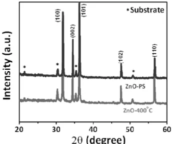
lapsing of the spherical voids after heat treatment. Other- wise, the films show solid interconnection among ZnO nanoparticles. The XRD patterns for ZnO and PS500-4 films after annealing at 400
oC are presented in Fig. 2, which confirms the hexagonal wurtzite phase of the ZnO particles in the films(JCPDS36-1451). No changes in the crystalline phase were observed when voids were inserted in the PS500 film, although the peak intensity slightly decreased possibly because of the generated voids.
The performance of the DSSCs fabricated using the electrodes having different void sizes were measured under illumination by a Sun 3000 solar simulator com- posed of a 1000 W mercury-based Xe arc lamp and AM 1.5 G filter. The photovoltaic parameters of open-circuit
voltage(V
oc), short-circuit current density(J
sc), fill factor (FF), and energy conversion efficiency( η) are summarized in Table 2 for the ZnO films dispersed under different void sizes. Generally, V
ocvalues were not noticeably different between the cells, because V
ocis mainly deter- mined by the energy difference between the Fermi level of ZnO and the redox potential of the electrolyte.
However, a significant difference was observed in J
scand FF. The highest efficiency was observed with the PS500 cell. The resonant scattering efficiently occurs when the size of scattering object is comparable with the wave- length of incident light.
19)Since the void volumes were controlled similar to the films, the highest short-circuit current of the PS500 cell resulted from the highest light scattering efficiency with the 500 nm-size voids.
3.2 The effect of void concentration to DSSC per- formance
To examine the effect of void concentration in the ZnO films, the amount of PS500 spheres was varied (0.0, 0.2, 0.4, and 0.8 g) for a fixed amount of ZnO (3.2 g). We call the films as ZnO, PS500-2, PS500-4, and PS500-8, respectively. The morphology of the films is shown in Fig. 1. FESEM images of ZnO films under different void sizes: a) ZnO (no voids), b) PS300, c) PS500, d) PS800, and e) PS1000, f) Cross- section of the PS500 film.
Fig. 2. XRD patterns of ZnO (annealed at 400
oC) and PS500 films.
Table 2. Photoelectric performance of the four cells with various PS diameters.
Working electrode
J
sc(mAcm
−2) V
oc(mV)
FF (%)
η (%)
PS300 9.32 615 48.54 2.78
PS500 9.38 630 56.87 3.36
PS800 8.9 625 57.18 3.18
PS1000 8.74 625 54.57 2.98
Fig. 3, where the void concentration increases according to the PS amount. The transmittance spectra of the photoanodes under different void concentrations were measured in the normal direction to the sample as shown in Fig. 4, and comparison with FTO glass substrate was also made. For ZnO having bandgap energy of 3.37 eV, the light absorption will be small for the wavelengths
less than > 370 nm.
20)However, Fig. 4 shows nearly full absorption at < 600 nm for a pure ZnO film made by agglomeration of nanoparticles about 100 nm in size. The transmittance at an infrared wavelength of 1000 nm was only about 20 %. Therefore, the particulate morphology of the film greatly promoted the light absorption in the long-wavelength regions. Notably, we observed that the reflection is negligible in the films.
21)The transmittance was further lowered to almost zero in the long-wavelength Fig. 3. FESEM images of ZnO films under different PS500 concentrations: a) zero, b) 0.2 g, c) 0.4 g, and d) 0.8 g.
Fig. 4. Light transmittance of photoanodes prepared using different PS concentrantions.
Fig. 5. The J-V characteristics of DSSCs fabricated with different
working electrodes.
region via inclusion of voids in the films, indicating that the spherical voids, each of about 500 nm in size, are highly efficient light-scattering centers leading to an en- hanced optical absorption efficiency of the film in the long-wavelength region.
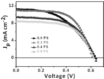
Fig. 5 compares the DSSC performance of the working electrodes under different void concentrations. The corres- ponding open-circuit voltages, short-circuit current den- sities, fill factors, and conversion efficiencies are presented in Table 3. The change in J
scis relatively large upon an increase of void concentration in the films, whereas changes in V
ocare relatively small. The decrease of the
current density with increasing void concentrations is brought by the decrease of the current path cross-section in the electrode. Meanwhile, the light absorption enhance- ment via enhanced scattering from the voids is already saturated with 0.2 g addition of the PS spheres, as shown in Fig. 4. In conclusion, the morphology of agglomerated nanoparticles already exhibited high light-capturing effi- ciencies, and the inclusion of voids further improved the efficiency via enhanced light scattering. However, degrad- ation of the current-carrying capacity of the electrode overrode the enhanced scattering effect at high void concentrations, where the optimized conversion efficiency obtained was 4.07 % for the PS2 electrode.
The electrochemical impedance spectra of the PS-series electrodes are shown in Fig. 6. The spectra were fitted to the equivalent circuit using the Z-view software. Table 4 summarizes the estimated values of the charge-transfer resistances of both counter and working electrodes, as well as the CPE parameters for the interfaces of both electrodes. To merely compare the working electrodes, four counter electrodes were fabricated using the same method and materials. None of the parameters for the counter electrode interface showed any significant differ- ence between the DSSCs. The Rct2 became small with increasing PS concentration from 0.0 g to 0.2 g, and Rct2 increased upon an increase in the PS concentration from 0.2 g to 0.8 g. The minimum Rct2 value of 4.55 Ω was obtained for the PS concentration of 0.2 g. A smaller Rct2 suggests longer electron lifetimes for power con- version efficiency
19)and decrease in total series resistance of the DSSCs.
2-4,17)The impedance spectra observations well coincide with the solar cell efficiency measurement results.
3.3 Effect of electrode thickness to the performance of DSSC
An optimum thickness of electrode film exists because of the trade-off between the carriers transport to the terminal and the light absorption by dyes. The thicker film thickness enhances the light absorption by dyes, but will also lead to a long carrier-transport length towards increasing recombination probability. Thus, the optimiza- tion process for the thickness of ZnO-PS electrode is Table 3. Photoelectric performance of the four cells shown in Fig. 5.
Working electrode
J
sc(mAcm
-2)
V
oc(mV)
FF (%)
η (%)
ZnO 11.25 635 47.29 3.38
PS2 11.04 610 60.39 4.07
PS4 9.38 630 56.87 3.36
PS8 8.47 620 58.71 3.09
Fig. 6. Nyquist plots of DSSCs for different photoanodes. The equivalent circuit diagram above is used to fit the observed impedance spectra. Abbreviations: R
h, ohmic serial resistance, Rct1, charge-transfer resistance of the counter electrode; CPE1: constant- phase element of the counter electrode; Rct2, charge-transfer resistance of the working electrode; CPE2, constant-phase element of the working electrode; W
s, Warburg impedance.
Table 4. Impedance parameters of four DSSCs under different photoanodes estimated from the impedance spectra and equivalent circuit shown in Fig. 6.
Working
electrode Rh ( Ω) Rct1 ( Ω) CPE1-T
(F) CPE1-P Rct2 ( Ω) Ws CPE2-T
(F) CPE2-P
R T P
ZnO 2.53 2.34 2.51E-05 0.93 5.05 1.59 0.79 0.5 3.73E-04 1.00
PS2 2.60 1.58 2.84E-05 0.93 4.55 1.45 0.88 0.5 3.88E-04 1.00
PS4 2.58 1.69 5.41E-05 0.86 6.02 2.04 0.78 0.5 3.06E-04 1.00
PS8 2.52 2.18 3.06E-05 0.93 6.62 2.24 0.78 0.5 3.88E-04 1.00
necessary. Fig. 7 shows the cross-section SEM images for various film thicknesses from 10 µm to 20 µm for a given PS500-4 photoanode structure. Fig. 8 shows the corresponding J-V characteristics of the DSSCs fabricated from the varying thicknesses, and Table 5 summarizes the measured V
oc, J
sc, FF, and η values. The thickness for the best DSSC performance was 12 µm for the efficiency of 4.07 %.
A DSSC fabricated with similar morphology of ZnO nanoparticles exhibited the highest efficiency of 5.61 %
at a thickness of about 26 µm.
8)This slightly higher efficiency was obtained with a little larger parameter values(V
oc, J
sc, and FF) from a much thicker film thick- ness than that from the experiment. We note in ref.
8)that the films had been fabricated with ZnO nanoparticles of 20 nm size,
21)which is smaller than < 100 nm we obtained from the experiment. Thicker films formed by smaller grains will provide a larger contact area with the dye molecules increasing the electron concentration injecting into the oxide particles. However, note that the morphology of fine grains would limit the absorption wavelength to relatively shorter wavelength region because scattering centers of hundreds of nanometer size are necessary for absorption of long wavelengths(Fig. 4). Fur- thermore, the long transport distance for the electrons to reach the external terminal as well as the large surface area would increase the recombination probability for the electrons. Therefore, we think the thin optimum film Table 5. Photoelectric performance of the four cells shown in Fig.
8.
Working electrode
J
sc(mAcm
−2)
V
oc(mV)
FF (%)
η (%)
10 µm 9.80 605 64.72 3.84
12 µm 11.04 610 60.39 4.07
15 µm 8.66 580 59.56 3.00
20 µm 7.50 520 57.08 2.23
Fig. 7. The cross-sectional of FESEM images of ZnO-PS films with different thickness.
Fig. 8. The J-V characteristics of DSSCs fabricated with different
thickness of working electrodes.
thickness in the study could be observed from the absorption of the entire wavelength range owing to the voids(Fig. 4); when all the light was absorbed on upper part of the film, the remaining lower part of the film simply enhances the recombination leading to a degrad- ation in the electrode performance. Therefore, our thinner film should show less carrier recombination rate than ref.
8)Our inferior efficiency observed was then due to the smaller electron concentration injected to the ZnO particles because of the coarseness of the particles. Therefore, employing much finer nanoparticles, each having a diameter of about 10 nm, may improve the efficiency. In addition, the detail material properties such as cry- stallinity of ZnO nanoparticles and/or other factors related with DSSC fabrication might not be rejected from the possible causes.
4. Conclusions
We fabricated working electrodes distributed with voids that serve as light-scattering centers to enhance light absorption, particularly in the long-wavelength region.
The performance of the electrodes was studied by fabrication of DSSCs and measuring the corresponding conversion efficiencies. The effects of the size and density of the spherical voids, and the film thicknesses were examined to obtain the optimal solar cell efficiency.
The void size of 500 nm was most effective in scattering sunlight for absorption enhancement in the long-wave- length region(> 600 nm). The highest overall conversion efficiency of 4.07 % was obtained from the photoelectrode of 12 µm thickness, PS sphere concentration of 0.2 g, and PS sphere diameter of 500 nm. An optimum film thickness was determined from a trade-off between the light scattering effect and electron transport efficiency for the optimum cell efficiency. The thin optimum film thickness was brought by a highly enhanced light absorp- tion for the entire wavelength region because of the voids distributed in the film. However, the enhanced light absorption was compensated by the small surface area of the used ZnO nanoparticles.
Acknowledgements
This research was supported by the National Research Laboratory and the Basic Research program(No. 2012R-
1A1A4A01011671) of the Ministry of Education, Science, and Technology of Korea.
References
1. B. O'Regan and M. Gratzel, Nature, 353, 737 (1991).
2. M. Grätzel, Inorg. Chem., 44, 6841 (2005).
3. V. -D. Dao, S. -H. Kim, H. -S. Choi, J. -H. Kim, H. -O.
Park and J. -K. Lee, J. Phys. Chem. C, 115, 25529 (2011).
4. V. -D. Dao, C. Q. Tran, S. -H. Ko and H. -S. Choi, J.
Mater. Chem. A, 1, 4436 (2013).
5. M. K. Nazeeruddin, F. De Angelis, S. Fantacci, A. Selloni, G. Viscardi, P. Liska, S. Ito, B. Takeru and M. Gratzel, J.
Am. Chem. Soc., 127, 16835 (2005).
6. M. Quintana, T. Edvinsson, A. Hagfeldt and G. Boschloo, J. Phys. Chem. C, 111, 1035 (2006).
7. Q. Zhang, C. S. Dandeneau, X. Zhou and G. Cao, Adv.
Mater., 21, 4087 (2009).
8. W. -C. Chang, C. -H. Lee, W. -C. Yu and C. -M. Lin, Nanoscale Res. Lett., 7, 1 (2012).
9. J. Ferber and J. Luther, Sol. Energy Mater. Sol. Cells, 54, 265 (1998).
10. M. Hamadanian, H. Sayahi and A. R. Zolfagharici, J.
Nanostructures, 1, 139 (2012)
11. Q. Zhang, T. P. Chou, B. Russo, S. A. Jenekhe and G.
Cao, Adv. Funct. Mater., 18, 1654 (2008).
12. M. Kevin, Y. H. Fou, A. S. W. Wong and G. W. Ho, Nanotechnology, 21, 315602 (2010).
13. C. H. Lee and H. W. Choi, Mol. Cryst. Liq. Cryst., 565, 124 (2012).
14. S. Hore, P. Nitz, C. Vetter, C. Prahl, M. Niggemann and R. Kern, Chem. Comm., 2011 (2005).
15. X. Sheng, J. Zhai, L. Jiang and D. Zhu, Appl. Phys. A, 96, 473 (2009).
16. H. N. Hieu, N. M. Vuong, H. Jung, D. M. Jang, D. Kim, H. Kim and S. -K. Hong, J. Mater. Chem., 22, 1127 (2012).
17. V. -D. Dao, H. -S. Choi and K. -D. Jung, Mater. Lett., 92, 11 (2013).
18. Q. Zhang, T. P. Chou, B. Russo, S. A. Jenekhe and G.
Cao, Ang. Chem. Int. Edit., 47, 2402 (2008).
19. S. Chang, Q. Li, X. Xiao, K. Y. Wong and T. Chen, Energy Environ. Sci., 5, 9444 (2012)
20. H. N. Hieu, N. Q. Dung, J. Kim and D. Kim, Nanoscale, 5, 5530 (2013).
21. H. N. Hieu, N. M. Vuong and D. Kim, J. Electrochem.
Soc., 160, H852 (2013).