Analyzing of CDTA using a New Small Signal Equivalent Circuit and Application of LP Filters
Junho Bang
1, Je-Ho Song
1*, Woo-Choun Lee
11Department of IT Applied System Engineering, Smart Grid Research Center, Semiconductor Design Education Center, Chonbuk National University
새로운 소신호 등가회로를 활용한 CDTA의 해석 및 저역통과 필터설계
방준호1, 송제호1*, 이우춘1
1전북대학교, IT응용시스템공학과, 스마트그리드연구센터, 반도체설계교육센터
Abstract A CDTA (current differencing transconductance amplifier) is an active building block for current mode analog signal processing with the advantages of high linearity and a wide frequency bandwidth. In addition, it can generate a stable voltage because all the differencing input current flows to the grounded devices. In this paper, a new small signal equivalent circuit is proposed to analyze a CDTA. The proposed small signal equivalent circuit provides greater precision in analyzing the magnitude and frequency response than its previous counterparts because it considers the parasitic components of the input, internal and output terminal. In addition, observations of the changes made in various devices, such as the resistor (Rz) confirmed that those devices heavily influence the characteristics of CDTA. The designed parameters of the proposed small signal equivalent circuit of the CDTA provides convenience and accuracy in the further design of analog integrated circuits. For verification purposes, a 2.5 MHz low pass filter was designed on the HSPICE simulation program using the proposed small signal equivalent circuit of CDTA.
요 약 CDTA는 전류모드로 아날로그 신호처리를 수행하는 능동회로로써 높은 선형성과 넓은 주파수 대역폭을 갖는 장점을 가지고 있다. 또한 입력 차동전류가 모두 접지된 임피던스 소자로 흐르게 되어 안정적인 동작을 수행하도록 한다. 본 논문에 서는 CDTA를 해석하기 위해 새로운 소신호 등가회로를 제안한다. 제안된 소신호 등가회로는 입력과 내부단자 및 출력단자 의 기생성분이 고려되어 크기 및 주파수 특성이 기존회로보다 정밀하게 분석될 수 있다. 제안된 소신호 회로를 활용하여 다양한 파라미터의 변화에 의하여 특성변동을 관찰한 결과, 저항(Rz) 등 특정한 값이 CDTA의 특성에 큰 영향을 주게 되는 것도 확인되었다. 본 논문에서 검증된 소신호 등가회로의 설계 파라미터는 CDTA 아날로그 회로와 그 응용회로를 설계하는 데 편리성과 정확성을 제공할 수 있음을 보였다. 본 논문에서 제안된 CDTA 소신호등가회로를 이용하여 2.5MHz 저역통과 필터를 설계하였고 HSPICE 시뮬레이션을 통하여 그 유용성을 검증하였다.
Key Words : Current mode, Lowpass filter, Small signal equivalent circuit, Transconductance amplifier
*Corresponding Author : Je-Ho Song (Chonbuk National University) Tel: +82-10-6630-6625 email: [email protected]
Received October 31, 2014 Revised (1st November 14, 2014, 2nd December 4, 2014) Accepted December 11, 2014
1. Introduction
Current differencing transconductance amplifier (CDTA), recently reported current-mode active
building block, appears to be very useful for current-mode signal processing. and its usefulness and popularity in analog integrated circuit design has been published in many papers [1], [2]. Using the CDTA
element, it is possible to obtain circuit solutions with less number of passive elements than its counterparts and it also leads to compact circuit structures requiring a few active building blocks in some applications. It has current as its input and the primary voltage can be obtained by the difference between two input currents. In here voltage is determined by the primary input node impedance and this voltage generates current through CDTA’s output with transconductance amplifier connected to the back-end.
CDTA can have high linearity and wide frequency bandwidth and being relatively small size circuit it can be used to design filters and analog circuits.
A simple form of small signal equivalent circuit is used[3]-[5] for modeling and analyzing CDTA. The existing equivalent circuits haven’t considered and analyzed the parasitic component which exists in the input, internal and output terminal of CDTA. A more precise equivalent circuit is necessary which can analyze the characterstics of CDTA even considering the parasitic components.
In this paper a new small signal equivalent circuit is proposed to analyze the characterstics of CDTA.
Considering the parasitic components the proposed circuit provides more precision in analyzing the magnitude and frequency response of the circuit also.
Chapter 2 shows all the input-output current and voltage characteristics of a CDTA using the proposed small signal equivalent circuit. Chapter 3 shows an application of CDTA in designing a 2.5 MHz low pass filter with HSPICE simulation results.
2. Small-signal equivalent circuit analysis of CDTA
The symbols and basic input-output voltage and current relationship of CDTA are shown in figure 1.
and are differencing current input signals which gets converted into voltage through the impedance in the node Z. The converted voltage signal gets convert into
currents and through transconductance.
(a)
(b)
[Fig. 1] (a) Symbols of CDTA, (b) Small-signal equivalent circuit of CDTA
(1)
[Fig. 2] Proposed small signal equivalent circuit of CDTA
For the detailed analysis of CDTA the small signal equivalent circuit is proposed as in the figure 2. The equivalent circuit of CDTA can be divided into current differentiator and transconductor. , and ,
are input impedance and , and ,
Device Value before adjustment
Value after adjustment
2pF 1pF
50 50
4.5pF 1pF
3M 10M
2pF 1pF
50 50
4.5pF 1pF
3M 10M
3.5K 3.5K
25pF 25pF
3.5K 3.5K
25pF 25pF
are output impedance of current differentiator. And
, and , are output impedance of transconductor. Here the differencing current can be shown as in the equation (2),
(2)
Here, b and c are current gain and error value, and d is the differencing current gain of and
respectively. The current error value of both Ip and In
takes the value of less than 1. At node z, external impedance value is connected when differencing input current is converted into voltage signal and thus the voltage obtained from node z is again converted into positive output current and negative output current through the
value. Here, the transconductance value “gm” can be adjusted through external biased current. Hence the output current also gets adjusted as it depends on the gm value. In order to design a circuit which is strong to noise characteristics generated in the fabrication process of integrated circuits, one of the important method is to construct all the devices of the passive circuit as grounded devices. Since, the z terminal of CDTA is grounded, it possess the characteristics of being strong to such noise. Using more than one grounded devices the differencing current can be converted to voltage since all the input differencing current flows to the z terminal. So small size circuits can be constructed using CDTA’s structural characteristics.
3. Design of LP filter using CDTA
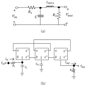
In this chapter, a passive lowpass filter is designed first and then a active lowpass filter designed through converting the passive filter with CDTAs. In a passive filter, an inductor can be easily replaced with another inductor composed of CDTA making the passive filter an active filter since CDTA is an active element[6-8].
(a)
(b)
[Fig. 3] (a) The desinged passive filter, (b) an active low pass filter.
Fig. 3(a) shows a second order passive filter and Fig. 3(b) shows active low pass filter made using CDTA. Here in the Fig. 3(a) represents the passive inductor which is designed using CDTA and in Fig. 3(b) it is implemented in the constructing an active low pass filter. Device values are given to the equivalent circuit in the figure 2 as shown in the table 1. Later considering these device values a second order low pass filter is designed.
[Table 1] Device values for the proposed small signal equivalent circuit
1mS 1mS
1mS 1mS
800 K 2M
Here, table 1 show before and after adjustment value of each elements of the proposed small signal equivalent circuit in Fig.2.
The changes in the characteristics of the low pass filter could be observed as the changes in the values of the designed parameters were made. Thus the optimal values of the devices composing the filter could be found.
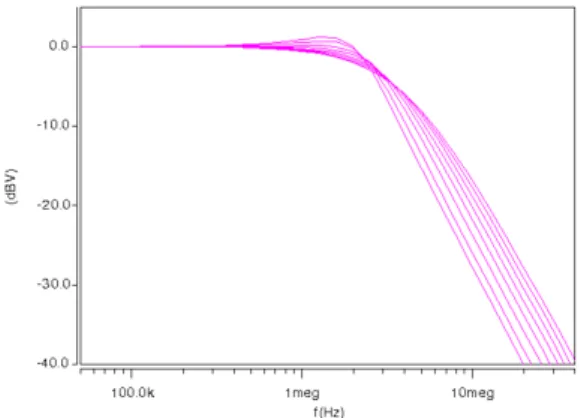
[Fig. 4] The center frequency of the active low pass filter by adjusting using the device values from Table 1.
[Fig. 5] The fixed center frequency to 2.5MHz of the active low pass filter
Figure 4 shows the change in the center frequency after adjusting values. The results of adjusting
from 400 to 1 and Rz of 2 show that
the center frequency of the designed filter can be adjusted by the device value which is extracted from the proposed small signal equivalent circuits. As a results, Figure 5 shows simulated result of low pass filter of 2.5 MHz center frequency with the fixed
of 1.
3. Conclusion
In this paper a new small signal equivalent circuit is proposed in order to analyze CDTA. The proposed circuit provides more precision in analyzing magnitude and frequency response than its previous counterparts since it considers parasitic components of the input, internal and output terminal. In addition to that, observing the changes made in various devices like resister(Rz), it has been confirmed that those devices heavily influence the characterstics of CDTA. The designed parameters of the proposed small signal equivalent circuit of the CDTA provides convenience and accuracy in the further design of analog integrated circuits. For the verification purpose, a 2.5 MHz low pass filter is designed using HSPICE simulation program using the proposed small signal equivalent circuit of CDTA.
And by using the extracted values and equivalent circuit of CDTA as proposed in this paper henceforth it is expected to be used in designing filters and analog integrated circuits.
References
[1] A.U. Keskin, D. Biolek, E. Hancioglu, E., and V.Biolkova,
“Current-mode KHN filter employing current differencing transconductance amplifiers”, AEU - International Journal of Electronics and Communications, Volume 60, Issue 6, 2006, pp. 443-446.
DOI: http://dx.doi.org/10.1016/j.aeue.2005.09.003
[2] A. Uygur and H. Kuntman, ‘Seventh order elliptic video filter with 0.1dB pass band ripple employed CMOS CDTAs’, AEU: International Journal of Electronics and Communications, Vol.61, 320-328, 2007.
DOI: http://dx.doi.org/10.1016/j.aeue.2006.06.002
[3] D. Biolek, “CDTA-Building block for current-mode analog signal processing”, Proc. ECCTD’03, Cracow, Poland, 2003, Vol. III, pp.397-400.
[4] D. Biolek and V. Biolkova, "CDTA-C current-mode universal 2nd_order filter", Proceeding of the 5th WSEAS International Conference on Applied Informatics and Communications, Malta, September 15-17, pp.411-414, 2005.
[5] F. K. Ar and H. H. Kuntman, "A new, improved CMOS realization of CDTA and its filter applications", Turk J Elec Eng & Comp Sci, Vol.19, No.4, 2011,
[6] W. Tanjaroen, T. Dumawipata, S. Unhavanich, W.
Tangsrirat and W. Surakampontorn, "Design of current differencing transconductance amplifier and its application to current-mode KHN biquad filter", Proceeding of ECTI-CON 2006, Ubon-ratchathani, Thailand, May 10-13, pp.497-500, 2006.
[7] A. lahiri, “Novel voltage current-mode quadrature oscillator using current differencing transconductance amplifiers”, Analog Integrated Signal Processing, Volume 61, pp.
199-203, 2009.
DOI: http://dx.doi.org/10.1007/s10470-009-9291-0 [8] Y. Anli, “Electronically turnable current-mode biquadratic
filter and four-phase quadrature oscillator”, Microelectronics Journal, Volume 45, pp. 330-335, 2013.
DOI: http://dx.doi.org/10.1016/j.mejo.2013.12.005
Junho Bang [Regular member]
•Feb. 1989 : Chonbuk National Univ., Department of Electric Engineering, B. S.
•Feb. 1991 : Chonbuk National Univ., Department of Electric Engineering, M.S.
•Feb. 1996 : Chonbuk National Univ.,Department of Electric Engineering, Ph. D.
•Mar. 1997 ∼ 1998 : LG Semiconductor Institute of Technology
•Mar. 1998 ∼ Current : Department of IT Applied System Engineering, Chonbuk National University, Professor.
<Research Interests>
Integrated circuit design of the analog and digital mixed mode signal processing.
Je-Ho Song [Regular member]
•Feb. 1991 : Wonkwang Univ., Department of Electronic Engineering, B. S.
•Feb. 1991 : Wonkwang Univ., Department of Electronic Engineering, M. S.
•Feb. 2003 : Wonkwang Univ., Department of Electronic Engineering, Ph. D.
•Mar. 1996 ∼ Current : Department of IT Applied System Engineering, Chonbuk National University, Professor.
<Research Interests>
VLSI, Information Communication, Communication Network System, and DSP design.
Woo-Choun Lee [Regular member]
•Feb. 1977 : Dankuk Univ., Department of Electric Engineering, B. S.
•Feb. 1985 : Myongji Univ., Department of Electric Engineering, M.S.
•Feb. 1995 : Myongji Univ., Department of Electric Engineering, Ph. D.
•Mar. 1992 ∼ Current : Department of IT Applied System Engineering, Chonbuk National University, Professor.
<Research Interests>
Electrical machine and Electrical control system