Ⅰ. Introduction
Power consumption is one of three factors which decides the circuit design efficiency together with cost and speed. In sub-micrometer transistors, researchers have been concerned very much in terms of leakage current consumption because transistor size is shrunk [1]. It leads to transistor density increase. Thus, it is a primary factor in increasing the power consumption, which includes dynamic power, static power and short-circuit power. Dynamic power and short-circuit power are collectively referred to as switching power and are consumed when the transistor switches states. Leakage power is consumed merely in the absence of switching activity.
As transistor size is shrinking more and more, the leakage current increases dramatically. Specially, leakage current becomes more important in
mobile applications and handheld devices where the battery lifetime is determined by the amount of power consumption. Reducing the leakage current is one of the most concerning problems in recent researches [2]. High leakage current affects seriously the consumption energy in sub-micrometer CMOS circuits.
Asynchronous circuit shows many advantages such as no clock skew, low power, easing of global timing issues, and so on [3]. Especially, asynchronous circuit design technique reduces dynamic power significantly due to its unlocked nature. In standby mode, switching power is not consumed due to no clock, however, the leakage current dissipation is comparable with the switching power [2]. Because asynchronous circuits eliminate the global clock which is used to capture and launch data, we need an extra circuit detecting the completion activity to realize analogous
Self-Power Gating Technique For Low Power Asynchronous Circuit
Kim-Ngan Thi Mai*, Huan Minh Vo*★
Abstract
In this paper, Asynchronous Self-Power Gating technique (ASPG) is used to reduce consumption power in asynchronous digital watch application. The power gating control signal is automatically generated by internal system operation characteristics instead of using replica circuit delay or four-phase handshaking protocol.
Isolation cell is designed to insert it between power gating domain and normal operation domain. By using self-power gating circuit, asynchronous digital watch application consumes very low power and maintains data during sleep mode. The comparison results show the proposed ASPG technique saves leakage power up to 40.47%
and delay time is reduced to 71% compared to the conventional circuit.
Key words:Power Gating, Self-Power Gating, Asynchronous Circuit, Leakage Current, Isolation Cell, Low Power
* Faculty of Electrical and Electronics Engineering, Ho Chi Minh Univeristy of Technology and Education
★ Corresponding author
E-mail:[email protected], Tel:+84-28-3896-8641
Manuscript received Aug. 8, 2018; revised Sep, 18. 2018; accepted Sep. 19. 2018
This is an Open-Access article distributed under the terms of the Creative Commons Attribution Non-Commercial License (http://creativecommons.org/licenses/by-nc/3.0) which permits unrestricted non-commercial use, distribution, and reproduction in any medium, provided the original work is properly cited.
27
functions. Usually, four-phase handshaking protocol and critical path replica delay line are used to implement asynchronous architecture design. The path replica delay line which consists of buffers in the series, is inserted into the pipelines to mimic the longest path delay for the combinational block. The delay line is deployed by an inverter chain to copy the critical path of the corresponding combinational block. This matched delay amount can be different depending on the length of pipeline.
Thus, the replica circuit must be designed accurately so that the setup time violation would not happen.
Actually, it is difficult to handle timing issues in designing the matched delay circuit. This requires a lot of experience and very accurate timing models. We need to develop accurate models to determine the length of the buffers. Besides, the impact of Process Voltage Temperature (PVT) variation affects the timing property. We also need to consider the random intra-die variation that results in deviation of timing parameters such as skew time, setup time and hold time.
Therefore, it is more difficult to satisfy these timing constraints in the replica circuit. Moreover, adding many buffers causes large switching and leakage energy penalties. The four-phase hand- shaking circuit builds handshaking protocol to communicate blocks each other. A local handshaking circuit controls system automatically in standby state when inactive. By sending the signals of request and acknowledgement, handshaking circuit activates the latch registers for data storage.
These request and acknowledgement signals enable switches to turn ON/OFF the combinational blocks which can be cut off supply power rail.
Thus, leakage current can be mitigated very much in standby mode [3].
Among various leakage reduction techniques, power gating is the most popular solution for efficient leakage power saving in both synchronous and asynchronous circuits [2] [4]. Power gating technique is developed to cut off this leakage in standby mode by turning off PMOS/NMOS
switches which are often used by high threshold voltage. By doing so, the supply power is turned off and the circuit is no longer consumed. The handshaking circuit detects the completion activity to control functions into standby mode. A replica timing circuit mimics the critical path delay of the combinational logic block correspondingly to make sure that power gating is implemented after logic blocks is going to idle state. The replica circuit depends on PVT variations of transistors seriously. It affects static timing analysis and causes inaccurateness in calculating circuit delay and power gating operation. To implement power gating technique in asynchronous circuit, the four-phase handshaking circuit creates an enabling signal from circuit operation conditions for saving power [5]. When the circuit is going to sleep mode, the enable signal is inactive, power gating switch is turned off. While the circuit is going to active mode, the enable signal is activated and turns on the circuit into normal operation. By doing so, the asynchronous power gating circuit needs an extra handshaking circuit which consumes more power dissipation and area overhead.
Using four phase handshaking circuit and the critical path replica delay circuit suffer disadvantages in term of power consumption, control complexity and area overhead. Creating internal control signals from internal function blocks can eliminate these troubles. Thus, the system switching power is reduced considerably because of getting rid of the extra circuits. A self-control signal generated from internal asynchronous blocks can be used to turn ON/OFF switches by power gating technique and moves the system into either sleep mode or active mode that depends on the system operation principle. It helps system optimize power saving.
In section II, the study creates the asynchronous self-control power gating signal and applies it to asynchronous digital watch application which is a clear example of asynchronous circuit with long standby time characteristics. Section III
presents asynchronous self-power gating technique to control lower power in asynchronous circuit.
Session IV analyzes simulation results. Session V is conclusion part.
Ⅱ. Asynchronous Digital Watch Design
The asynchronous digital watch application is a specific type of asynchronous counter, independent on clock pulse, no clock skew resulting in saving power a lot. The digital watch shows time range from 0 hours 0 minutes 0 seconds (00:00:00) to 23 hours 59 minutes 59 seconds (23:59:59), then keeps repeating.
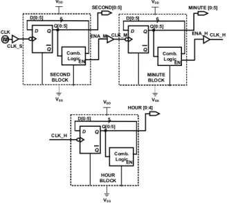
Figure 1 shows the asynchronous circuit schematic of the second timer block, minute timer block and hour timer block. The schematic includes modulo-60 counter for second timer and minute timer, modulo-24 counter for hour timer. At CLK falling edge, the second timer counts from 0 to 59. At the 59th second, ENA_M output becomes a high level logic and moves to a low level logic at next CLK which enables minute counter start counting. As the same way as second timer, the minute timer counts from 0 to 59 at the CLK_M falling edge. At the 59th minute, ENA_H output becomes high and moves to a low logic level at next CLK_M which creates CLK_H clock to
enable the hour counter active as shown in figure 1. The asynchronous digital watch circuit will reset to 0 hours 0 minutes 0 seconds after counting to 23 hours 59 minutes 59 seconds in the next CLK clock cycle.
Ⅲ. Power Gating in Asynchronous Circuit
A. Power Gating technique using single NMOS In this part, power gating concept is presented to clarify the advantage in reducing leakage current in sub-micrometer designs.
Figure 2 describes power gating technique using single NMOS transistors. Figure 2a shows an NMOS switch is inserted into the digital logic block. Here, the NMOS transistor plays a role as a switch to turn ON/OFF supply power rail.
This switch often uses high threshold voltage transistors to reduce leakage current. When the circuit is active, the Enable signal is logic 1. The NMOS transistor is ON. The VVSS node is discharged to 0 V. When the circuit is in inactive, the Enable signal is logic 0. The NMOS transistor is OFF. The VVSS node is charged to nearly VDD. A current portion is leaked through NMOS to ground [1]. The figure 2b shows corresponding waveform to nodes in figure 2a.
Comb.
Logic VDD
VSS Enable VVSS
(a) (b)
Active
Sleep Sleep
Enable VDD
VVSS
(a) NMOS power gating for combinational logic (b) node waveform
Figure 2. Power gating technique with single NMOS.
Normally, the combinational logic block is supplied with full VDD in normal operation because the NMOS switch is turned on. When a combinational logic block is active, it consumes
CLK CLK_S
ENA_M
SECOND BLOCK
VDD
VSS 6
SECOND[0:5]
Comb.
Logic Q Q D Q[0:5]
D[0:5]
EN
ENA_H
MINUTE BLOCK
VDD
VSS 6
MINUTE [0:5]
Comb.
Logic Q Q
D Q[0:5]
D[0:5]
EN CLK_M
HOUR BLOCK VDD
VSS 5
HOUR [0:4]
Comb.
Logic Q Q
D Q[0:5]
D[0:5]
EN
CLK_H
CLK_H
Figure 1. The asynchronous digital watch circuit consists of second timer, minute timer and hour timer.
the switching power in active mode. After the switching moment, the block continues leaking current during idle state. Thus, the power gating will mitigate this leakage current to save power loss.
B. Isolation cell
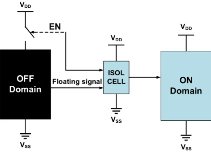
Power gating increases the delay timing and causes floating output in standby mode. Here, floating signal, which is not high logic, but also not low logic specifically, gets undetermined voltage affecting the normal operation. Isolation cells are designed to tie its floating point to a specific voltage. The isolation cell is designed to reduce the short circuit current due to floating nodes [4]. The isolation cell includes three types of forcing logic 0, logic 1 and holding the current state. In this paper, an isolation cell is designed to prevent floating voltage by forcing the node to logic 0.
Figure 3 describes the isolation cell circuit. The floating signal from the OFF domain will be connected to the ISOL block. The floating signal passing through the ISOL block will achieve a defined logic level of 0 or 1 that is the input to the ON domain. Here, the EN signal is used to control power gating switch to turn ON/OFF the circuit. Thus, the OFF domain is switched back and forth between operation and sleep mode.
OFF
Domain ON
Domain
ISOL CELL Floating signal VDD
VDD
VDD
VSS
VSS
VSS
EN
Figure 3. The function of the isolation cell.
An isolation cell can hold a defined logic level (logic 0 or 1), or it can hold the current value of the signal. Normally, simple logic gates like OR, AND, or a latch circuit can be used as an isolation cell at the output. An isolation cell circuit shall be designed with the proposed power gating circuit which isolates the active and inactive domain to keep the signal state without floating.
Figure 4 describes isolation cell in forcing logic 0. Figure 4a depicts scheme of AND gate in function of an isolation cell. The EN signal controls an operation circuit. When the EN signal is low, the output is low regardless of the IN input state. Here, the input signal is floating node which is sent from the OFF domain output.
When the EN signal is high, the circuit operates as a buffer gate. The input signal is transferred transparently to this buffer gate output. When the OFF domain is moved to a normal operation condition, its output will be sent to a specific voltage signal. As a result, the OUT signal is achieved as buffer gate output. When the OFF domain is turned off, the OUT signal also keeps at 0 V constantly. Noted that the isolation cell is always supplied full VDD to isolate the OFF domain and ON domain. Figure 4b describes isolation cell waveform. The EN signal is used to control the isolation cell. The IN signal is from the combinational logic block output.
When Combinational Logic block is turned off, its output is floating. Consequently, the ENA_M_PG signal will be logic 0 regardless of EN signal as shown in figure 4. At the falling edge of the 59th second pulse, ENA_M becomes a logic 1 and falls down logic 0 after 0th second pulse. This ENA_M is used to activate the minute timer in the conventional circuit. Noted that the ENA_M_PG signal is implementation result of the AND isolation gate between CLK and ENA_M. Thus, ENA_M_PG pulse only rises and falls during high levels of CLK as in figure 4.
C. Asynchronous Self-Power gating technique and isolation cell in asynchronous digital watch application
VDD
VSS
IN EN
OUT
(a) (b)
58 59 0 1
CLK (EN) ENA_M (IN)
ENA_M_PG (OUT)
(a) Isolation cell circuit
(b) The waveform node of isolation cell Figure 4. Isolation cell keeps logic 0 using AND gate.
Basically, the proposed asynchronous digital watch is similar to conventional one in operation principle as shown in session II. In this part, the proposed one uses an NMOS transistor as a switch and the isolation cell to prevent floating node phenomenon. Because the combinational logic block consumes much power in operation state, the power gating technique mitigates this consumption to save power loss in idle state.
When doing power gating, the combination logic block output will be floating which affects the shutdown domain next to power-on domain. To overcome this floating problem, the isolation cell is used to lead floating signal to logic 0. The advantage of the proposed ASPG technique is to use the internal control signals created from the timer block. Thus, the system does not use an external signal from power management block to do power gating.
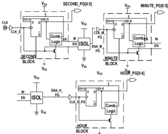
Figure 5 describes the asynchronous digital watch circuit combining the ASPG technique and the proposed isolation cell. In second timer block, the CLK signal is used as a clock pulse for D flip-flops that are always power-on. Simultaneously, the CLK signal also controls NMOS power gating switch and isolation cell (ISOL). When a CLK signal is rising, the NMOS switch is ON.
Thus, the Comb.Logic block creates D signal to
D-Flip flops in normal operation. The EN signal is used to be ISOL block input. The D signal is shifted to the Q output at the CLK falling edge.
In this case, the ISOL block plays a role as a buffer which transfers the ENA_M_PG signal to become the minute timer CLK_M_PG. When the CLK edge is falling down, the NMOS switch is OFF. Thus, the Comb.Logic block output of second timer will be floating due to power down.
In case of applying power gating, the ISOL block uses AND gate to isolate floating nodes by tying it to 0 volts.
CLK
VDD
VSS
ISOL
MINUTE BLOCK
VDD
VSS 6
MINUTE_PG[0:5]
Comb.
Logic
Q Q D Q[0:5]
D[0:5]
VDD
VSS
ISOL SECOND
BLOCK VDD
VSS 6
SECOND_PG[0:5]
Comb.
Logic
Q Q D Q[0:5]
D[0:5]
EN CLK_S
IN
EN ENA_M_
PG CLK_M_
PG EN IN
EN
HOUR BLOCK
VDD HOUR_PG[0:4]
Comb.
Logic
Q Q D Q[0:4]
D[0:4]
CLK_H_PG ENA_H_
PG
5 IN
EN
Figure 5. An asynchronous digital watch circuit using proposed ASPG technique and isolation cell.
Similarly to minute timer block and hour timer block, the EN output of minute timer is leaded to ISOL block and controlled by previous CLK_M_PG.
The ISOL cell will tie the Comb.Logic block output to 0 V if it is going to sleep mode. In active mode, the ISOL cell will transfer the input signal to output as a buffer. The D signal is shifted to the Q output at the clock falling edge.
The Flip Flops of the timers are always power-on. Thus, they maintain Q output data even if power gating occurs to Comb.Logic block. This signal is only transferred from the D input to Q output when there is a clock falling edge. Thus, undefined value nodes do not pass through these flip flops.
CLK_H_PG
58 59 0 1
CLK
58 59 0 1
CLK_M_PG 59 0
CLK_H
58 59 0 1
CLK
58 59 0 1
CLK_M 59 0
(a)
(b)
Figure 6. Clock signal of the asynchronous digital watch circuit. (a) Clock waveform in the conventional asynchronous digital watch circuit. (b) Clock waveform in the proposed digital watch with asynchronous self-power gating (ASPG) technique.
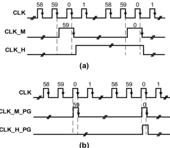
Figure 6 describes clock waveform for minute timer block, hour timer block. The figure 6a shows clock signals for the conventional asynchronous digital watch. When there is a falling edge of the 59th CLK, CLK_M signal reaches high level and returns to low level at the next CLK clock falling edge. Similarly, CLK_H signal rises to a high level at the 59th CLK_M and turns back to a low level at the next CLK_M clock falling edge. As shown in figure 6a, the CLK_M will slightly delay in comparison with CLK. The CLK_H is also a little bit later than the CLK_M due to logic propagation delay. The Figure 6b shows the waveform of CLK, CLK_M_PG and CLK_H_PG signals in the ASPG circuit which are used in both roles of capturing data and enable signal for doing power gating. In this proposed asynchronous power gating circuit, the ASPG technique together with proposed isolation cell does not only reduce data loss, but also retains output data during power-off duration.
When the 59th CLK edge falls down, the CLK_M_PG still keeps at low level at current CLK cycle. Here, CLK_M_PG still stays low until the next CLK cycle. At the beginning of
60th CLK falling edge, meaning 0th CLK falling edge, the CLK_M_PG gets the effect of ISOL block. Here, CLK_M_PG signal is flipped to high logic and low logic only during a CLK cycle.
When the 59th CLK signal switches up to high level and down to low level, the CLK_M_PG signal is still kept low due to effect of passing ISOL block. It is only up to high levels when detecting the rising edge of next CLK as in figure 6b. As a consequence, it allows the minute timer to increase the sleeping duration which results in more efficient power savings. The signal delay will depend on the CLK pulse cycle as a result of AND isolation gate. Thus, the proposed circuit will operate faster than the normal asynchronous circuit. Similarly, the CLK_H_PG signal only becomes a high level when the CLK_M_PG is going to be a high level at 60th CLK_M_PG pulse as shown in figure 6b.
Ⅳ. Simulation Results
In this paper, the leakage current reduction circuit is designed by Cadence software and DC compiler tool with 45nm technology [6]. The basic circuit diagrams are presented in Figure 2 and Figure 5 in Part III.
A. Wake-up time comparison
The wake-up time is transition time from sleep state to an active state, which is a quite important metric in power gating designs. The wake-up time is usually measured by the time interval between 10% VVSS value or 90% VVDD
value in comparison with the 50% clock value.
When changing the size of the NMOS switch, the circuit delay will be varied. Thus, the NMOS switch size is chosen to satisfy the design constraints. Figure 7 shows the wake-up time curve of the circuit blocks when changing the NMOS transistor width. The smaller NMOS transistor size, the larger delay time. In this paper, the wake-up time is measured by the
difference between 10% VVSS value and 50%
clock pulse. The total width size of the design circuit is 60μm for the mod-60 block, 30.33μm for the mod-24 block. The NMOS switch size is selected at 6μm for the mod-60 block and 3.3μm for the mod-24 block. It means that switch width is about 10% total size of the mod-60 block and mod-24 block for doing power gating technique.
Choosing the NMOS transistor size depends on the purpose of the application constraints such as speed, power consumption and area overhead.
Additionally, the ISOL cells have occupied approximately 2% more overhead area compared to the total area. Hence, the overhead area of the proposed circuit is 12% larger than the conventional circuit.
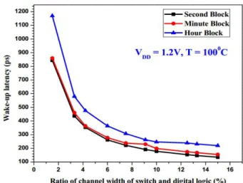
Figure 7. Wake-up time comparison for the second, minute, hour timer at 270C, 1.2V supply voltage.
As shown in figure 7, the wake-up time of the second, minute, and hour timer blocks can be analyzed when resizing the NMOS switch at 270C.
Figure 8 shows the results of the wake-up time comparison with the various timer blocks when changing the NMOS switch size at 100oC.
The wake-up time increases as the temperature rises and the mobility of the transistor decreases.
Figure 8. Wake-up time comparison for second, minute, hour timer blocks at 100oC, 1.2V supply voltage.
B. Delay time comparison
Figure 9 shows the clock delay time in the conventional circuit and the proposed ASPG circuit. At the falling edge of the 59th clock, the CLK_M and CLK_OUT1 output will go high and low until the 0th CLK. The CLK_M, CLK_OUT1 and CLK_M_PG will be delayed a little time compared to original CLK pulse. The cause is due to the propagation delay of the flip flops and logic gates of the timer blocks. Particularly, the power gating circuit latency will increase owing to influence of the NMOS switch width. Let t1be the delay time of the conventional circuit and t2
is the delay time of the circuit using the ASPG technique, we have t2> t1. The CLK is used as the control signal in an isolation cell. When detecting pulse edge, the input signal is converted to the ISOL block output. When there is no CLK pulse, the output will always be kept at 0 volts, which gives the CLK_M_PG output signal a much smaller t3 than t1, delay of the conventional circuit.
58 59 0 1
t3
CLK
t1
t2
CLK_M
CLK_OUT1
CLK_M_PG
Figure 9. The clock delay in the conventional circuit compared with asynchronous power gating circuit.
Table 1 shows the latency difference between the conventional circuits and the ASPG circuit at 27oC and 100oC. The ASPG-based circuit has 71% clock delay reduction compared to the conventional circuits at 27oC. In particular, the ASPG-based circuit is 73% less clock delay compared to the conventional circuits at 100oC.
Table 1. The clock pulse delay in the conventional asynchronous digital watch circuit and ASPG-based circuit at 27oC and 100oC.
Temper-at- ure
Minute timer delay (ps)
Hour timer delay (ps) The
Conventional
270C 71.248 144.037
1000C 106.116 214.406
ASPG 270C 20.312 41.698
1000C 28.468 58.562
C. Energy consumption comparison
The energy saving comparison is analyzed in Section III. Table 2 shows the power consumption of the second timer block during sleep time at 27oC and 100oC. Here, P1 is the consumption power of the conventional circuit and P2 is the consumption power of the ASPG circuit. Sleeping time is the time interval that the circuit is in standby mode. The power consumption is mainly the leakage power in case of longer sleep time because the active time is very short. The switching power causes significant increase in total consumption power. If the sleep time is short, the ASPG technique is more energy consumption than conventional circuits. Therefore, it has better not use ASPG technique in case of short sleep time. As the temperature rises, the leakage power increases dramatically as in Table 2. When the sleep time is less than 15μs, the ASPG power consumption is greater than the conventional circuit. Specifically, when the sleep time is 0.1μs, the ASPG circuit consumes 4.41μW whereas the conventional circuits consume only 4.16μW at the same temperature of 27oC.
Table 2. Consumption power of the second timer in the conventional circuit and ASPG circuit at 270C and 1000C during sleep time.
Temper ature
Sleep
time(µs) 0.1 1 5 10 50 90
270C P1(µW) 4.16
P2(µW) 4.41 4.4 4.32 4.22 3.44 2.67
1000C P1(µW) 13.04
P2(µW) 13.3 13.3 13.0 12.7 10.4 8.04
At a temperature of 27oC, the ASPG-enabled circuit saves up to 35.8% consumption power compared to the conventional circuit at 90µs sleep time. Meanwhile, at 100oC, the ASPG circuit saves up to 38.3% consumption power at the 90µs sleep time.
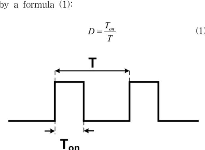
As shown in Table 2, increasing sleep time achieves the benefits of power saving. Figure 10 depicts the clock cycle. Where T is the pulse cycle, Ton is the time that the pulse stays high.
Duty cycle is the ratio of high voltage pulse time to pulse cycle T. Duty cycle (D) is determined by a formula (1):
Ton
D= T (1)
T
Ton Figure 10. Clock duty cycle.
Table 3 shows the ASPG technique is much more energy efficient than the conventional circuits at 27oC. The power consumption of the conventional circuit is almost independent on the duty cycle. Meanwhile, the clock duty cycle will affect the power consumption of the ASPG circuit. The smaller duty cycle, the longer sleep time, the less power consumption circuit. The
larger duty cycle, the shorter sleep time, the more power consumption circuit.
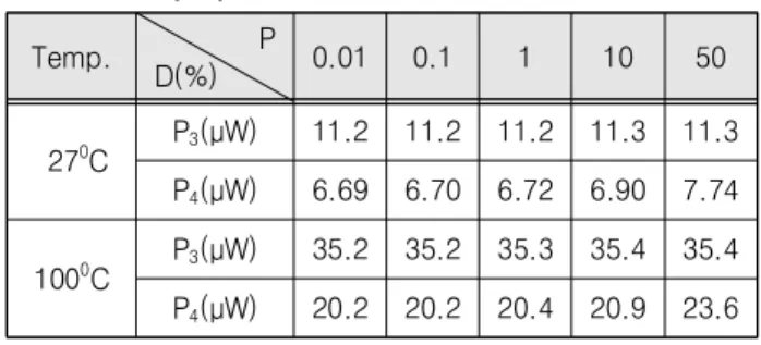
Table 3. The average power consumption of the conventional and the ASPG circuit when the duty cycle is varied at 27oC and 100oC.
Temp. P
D(%) 0.01 0.1 1 10 50
270C P3(µW) 11.2 11.2 11.2 11.3 11.3 P4(µW) 6.69 6.70 6.72 6.90 7.74
1000C P3(µW) 35.2 35.2 35.3 35.4 35.4 P4(µW) 20.2 20.2 20.4 20.9 23.6
The various duty cycles are simulated for fair comparison results in Table 3. At 27oC, the ASPG circuit with 1% duty cycle is 6.72μW in average power consumption. As the temperature increases, the consumption power increases dramatically. At 100oC, the ASPG circuit with 1% duty cycle is 20.4μW in the average consumption power. The P3 is the consumption power of the conventional circuit. The P4 is the consumption power of the ASPG circuit. The ASPG circuit power will decrease as the duty cycle decreases. The power value will be saturated and not be reduced further even if the value of the duty cycle continues to decrease.
This reason is because leakage power is a dominant component in total circuit power when sleep time is long enough. It will remain stable throughout the rest of sleep time. When the duty cycle is 0.1%, dominant part of power loss is only the leakage power. If the duty cycle continues to decrease, the power consumption level remains unchanged.
Ⅴ. Conclusion
Asynchronous Self Power Gating technique is very beneficial in terms of power saving and latency. The ASPG based circuits have achieved 40.47% power savings and 71% less latency compared to the conventional technique at 1%
duty cycle and 27oC. At 100oC, the circuit saves 42.24% the consumption power and 73% delay in the 1% duty cycle. The ASPG technique shows that it saves consumption power and improves the delay time more than the conventional circuit.
The improvements extend the battery lifetime of existing electronic devices such as mobile phones, laptops, tablets. The system advantage is to use control signals that are automatically generated from internal function blocks although it spends a little area overhead.
References
[1] Akhila Abba, K Amarender, “Improved Power Gating Technique for Leakage Power Reduction,”
Research Inventy: International Journal Of Engineering And Science, Vol.4, No.10, pp.06-10, Oct. 2014.
[2] Huan Minh Vo, Chul-Moon Jung, Eun-Sub Lee, and Kyeong-Sik Min, “Dual-switch power gating revisited for small sleep energy loss and fast wake-up time in sub-45-nm nodes,” IEICE Electronics Express, Vol.8, No.4, pp.232-238, Feb.
2011. DOI:10.1587/elex.8.232
[3] Ik Joon Chang, Sang Phill Park, and Kaushik Roy, “Exploring Asynchronous Design Techniques for Process-Tolerant and Energy-Efficient Subthreshold Operation,” IEEE Journal Of Solid-State Circuits, Vol.45, No.2, pp.401-410, February 2010.
DOI:10.1109/JSSC.2009.2036764
[4] Yvain Thonnart, Edith Beigné, Alexandre Valentian, and Pascal Vivet, “Power Reduction of Asynchronous Logic Circuits Using Activity Detection,” IEEE Transactions On Very Large Scale Integration (VLSI) Systems, Vol.17, No.7, pp.893-906, July 2009. DOI:10.1109/TVLSI.2008.2011912 [5] Chong-Fatt Law, Bah-Hwee Gwee, and Joseph S. Chang, “Modeling and Synthesis of Asynchronous Pipelines,” IEEE Transactions On Very Large Scale Integration (VLSI) Systems, Vol.19, No.4, pp.682-695, April 2011. DOI:10.1109/TVLSI.2009.2039501
[6] Predictive Technology Model (PTM) at http://ptm.asu.edu.
BIOGRAPHY
Huan Minh Vo (Member)
received the B.S. and M.S.E.E.
degrees in Electronics and
Communication Engineering from the Ho Chi Minh City.
University of Technology, Vietnam in 2005 and 2007. and Ph.D. degree in Electronics Engineering from Kookmin University, Seoul, Korea in 2013.He is currently working as a lecturer at the Faculty of Electrical and Electronics Engineering, University of Technology and Education, Ho Chi Minh City, Vietnam. His current research interests include low power design optimization and neuromorphic computation using emerging technology like memristive devices.
Kim-Ngan Thi Mai (Member)
received the B.S degree in Telecommunication Technology Engineering from University of Technology and Education.
Ho Chi Minh City, Vietnam in 2017. She has worked as a hardware designer at Microchip Technology Company, Vietnam so far. Her current research interests include lower power design optimization and physical design.