1. Introduction
Nano-structure Si solar cells have been extensively investi- gated for their high conversion efficiency. The optical layer of Si nano- structures with surface plasmon waves plays an important role in enhancing light absorption in a broad spectral range that gives rise to photo-current response and increases the performance of solar cells
1,2).
For surface plasmon effect, Ag is widely used for its low absorption losses whereas Au can be used in order to obtain high efficiency
3). Nano-particles of Ag and Au have plasmon resonances at 350 and 480 nm respec- tively, and these plasmon resonances can be red-shifted by embedding in Si at a spectral wavelength range of 500 to 1500 nm
4). Furthermore, Au nano-particles have a lower frequency resonance than Ag nano-particles. Alloying two metals of different ratios can create resonances between nano-particles, but these can be controlled using nano-shells. The red-shifting of resonance leads to enhancement scattering at longer wave- lengths which is beneficial for high light absorption in Si solar
cells
5, 6).
The melting points of Au and Si are 1064 and 1414 ℃, respectively, whereas the melting point is only 363℃ in the eutectic point case according to the phase diagrams of binary Au alloys of Massalski
7). Au silicide formation occurs at this low annealing temperature. The interaction between Au and Si leads to the formation of the alloy Au silicide, and it is also known that Si alloy with Au forms the eutectic alloy temperature, which can be used as low melting point solder of an Si transistor device
8-10).
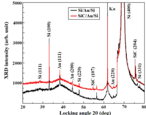
In this work, we investigated eutectic effects on Au thin film for the formation of Si nano-structures. The fabricated small Si and Si carbide(SiC) nano-particles were coated and biased on textured p-n junction Si solar cells, respectively. Then, Au thin film of 10 nm and Si thin film of 100 nm were deposited on the samples. The Si and SiC nano-particles and Au thin film were structurally embedded in Si thin films, but Au silicide nano- balls were formed by the eutectic bonding of Au and Si during the hot wire chemical vapor deposition(HWCVD) process of the substrates pre-heated temperature of 450℃ on the Si thin film surface. Various formations of nano-structures and balls were formed depending on the deposited metal and Si surfaces.
Eutectic Temperature Effect on Au Thin Film for the Formation of Si Nanostructures by Hot Wire Chemical Vapor Deposition
Hyung Yong Ji
1)․ Bhaskar Parida
2)․ Seungil Park
1)․ MyeongJun Kim
1)․ Jong Hyeon Peck
1)․ Keunjoo Kim
2)*
1)
Energy Conversions Technology Center, Korea Institute of Industrial Technology, Cheonan 331-825, Korea
2)


![외국인 PCR검사 가능 기관 [Referral Laboratories : 11sites]](data:image/gif;base64,R0lGODlhAQABAIAAAP///wAAACH5BAEAAAAALAAAAAABAAEAAAICRAEAOw==)