Journal of the Korean Crystal Growth and Crystal Technology Vol. 22, No. 1 (2012) 15-18
http://dx.doi.org/10.6111/JKCGCT.2012.22.1.015
Effect of annealing temperature on amorphous indium zinc oxide thin films prepared by a sol-gel spin-coating method
Sang-Hyun Lee, Seung-Yup Lee and Byung-Ok Park†
Department of Inorganic Materials Engineering, Kyungpook National University, Daegu 702-701, Korea (Received October 21, 2011)
(Revised November 22, 2011) (Accepted December 2, 2011)
Abstract Transparent conductive indium zinc oxide thin films were prepared by spin-coating a sol-gel solution. Zinc acetate dihydrate [Zn(CH3COO)2· 2H2O] and indium acetate [In(CH3COO)3] were used as starting precursors, and 2- methoxyethanol with 1-propanol as solvents. Upon annealing in a temperature range from 500 to 1000oC, the thin film crystallizes into polycrystalline In2O3(ZnO). The lowest electrical resistivity was obtained at an annealing temperature of 700oC as 2Ω · cm. Average optical transmittances were higher than 80% at all annealing temperatures. These experimental results confirm that the sol-gel spin-coating can be a good simplified practical method for forming transparent electrodes.
Key words Sol-gel, Indium-zinc oxide, Electrical properties and measurements, Optical properties
1. Introduction
Transparent conducting oxide (TCO) thin films have received extensive attention because of their diverse applications as transparent electrodes for optoelectronic devices such as flat panel displays and solar cells.
Among the TCO films, ITO is well known as the most commonly used materials because of low resistance and high optical transparency. However, Superior character- istics to improve the electrical conductivity of ITO films were chosen instead of the IZO. Recently, indium-zinc oxide [1-7] and numerous studies have shown. In partic- ular, Moriga et al. [1] revealed nine homologous com- pounds of In
2O
3(ZnO)
kcomposition (k = 3, 4, 5, 6, 7, 9, 11, 13 and 15).
Usually, IZO thin films were prepared by a pulsed laser deposition (PLD) [3-5] or magnetron sputtering method [6, 7]. In these ways, highly c-axis oriented and well crystallized thin films were obtained. However, it was difficult to obtain such well crystallized thin films from sol-gel spin-coating method [8, 9]. We revealed in our former paper [10-13] that the crystallized IZO films showing a strong orientation along c-axis can be achieved by extremely decreasing the solution concentration. How- ever, the crystallized thin films prepared by sol-gel spin- coating have not possessed better properties than amor-
phous films, rather worse properties. Thus, not crystal- line films but amorphous films needed to be investigated.
In this work, we studied the effects of annealing temper- ature on the IZO films whose crystal structure was amorphous.
2. Experimental
Indium solution and zinc solution were separately prepared in order to prepare a clear starting solution for IZO film, and then the two solutions were mixed. First, the indium solution was prepared. Indium acetate (In(CH
3COO)
3) was dissolved in 1-propanol by stirring the solution at 85
oC for 1 hour. Diethanolamine (DEA) was added as a stabilizer. The molar ratio of DEA/In was 1.5. Second, zinc acetate dihydrate (Zn(CH
3COO)
2· 2H
2O) was used as precursor material for the zinc solu- tion. The zinc acetate dehydrate and monoethanolamine (MEA) were dissolved in 2-methoxyethanol, and the solution was stirred at 50
oC for 40 min. The molar ratio of MEA (stabilizer) to Zn was the unity. Third, the indium and zinc solutions were mixed and stirred at room tem- perature for 2 hrs and finally, the starting solution (0.06 M) for the thin films was completed.
The starting solution for IZO film was dropped onto quarts glass substrate (15 × 15 × 1 mm) and rotated at 3000 rpm for 30 sec. The substrate was cleaned in an ultrasonic bath with acetone, ion exchanged water, and ethanol successively. After each coating process by spin-
†Corresponding author
†Tel: +82-53-950-5634
†Fax: +82-53-950-5645
†E-mail: [email protected]
16 Sang-Hyun Lee, Seung-Yup Lee and Byung-Ok Park
ning, the coated layer was pre-annealed at 400
oC for 10 min on a hot plate. The process from coating to pre- annealing was repeated for the desired thickness (approxi- mately 250 nm). The films were then annealed in an electric furnace.
The structural property of the films was analyzed using X-ray diffractometer (XRD) with CuK
α radiationoperated at 40 kV, 30 mA. The microstructure of the films was examined by scanning electron microscopy (SEM) at 20 kV. The electrical properties such as the resistivity, the carrier concentration, and the Hall mobil- ity were determined by measure by using a four-probe van-der-Paw technique. Optical transmittance was mea- sure by an ultraviolet visible near-infrared spectropho- tometer.
3. Results and Discussion
Figure 1 shows the XRD patterns of the IZO thin films at various annealing temperatures. An amorphous phase with a broad diffraction peak at 2
θ = 30~37owas observed from 400 to 700
oC. As the temperature increased, the main peak of indium oxide appeared at 2
θ = 30.6o. Moreover, the broad peak (2
θ = 30~37o) became
rather higher with temperature. This might be because the IZO simultaneously including diverse compositions werea on the way to crystallize [3]. In fact, most of the strong peaks from diverse compositions of indium zinc oxides were located between 30 and 37
o[1]. Consider- ing the frequency of the strong peaks found in the range, it was quite plausible that the broad peak was shaped like a wedge.
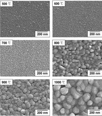
The microstructure of the thin films was shown in Fig. 2. There was a distinct difference in grain size between 500~700
oC and 800~1000
oC. The grain size was 10~20 nm in the range of 500 to 700
oC without conspicuous increase. As the temperature increased, the grain size suddenly increased to 90~130 nm at 800
oC and then 150~270 nm at 1000
oC.
Figure 3 shows the dependence of electrical proper- ties on the annealing temperature. At all temperatures, there was not significant change in mobility. The incre- ment of the grain size in the range of over 800
oC did not contribute to the increase of mobility. Maybe, this was because diverse compositions of the phases were blocking free electrons. The carrier concentration increased sharply and has the maximum value at 700
oC, and then started to decrease. Free carriers of IZO originate from donor sites associated with oxygen vacancies [14], so that the curve of the carrier concentration could be explained by oxygen vacancies. Adsorbed oxygen atoms
Table 1The results of Hall measurement IZO thin films with post- annealing treatment
Post-annealing conditions ρ (cm) n (cm−3) µ (cm2/Vs) No post-annealing 0.14 5.65 × 10¹⁸ 7.95 Inert atmosphere (N2) 0.05 1.12 × 10¹⁹ 10.6 Reducing atmosphere (N2+ 6 %H2) 0.02 3.26 × 10¹⁹ 9.87
Fig. 1. The XRD patterns of indium zinc oxide films with annealing temperature.
Fig. 2. The surface morphologies of the thin films with annealing temperature.
Effect of annealing temperature on amorphous indium zinc oxide thin films prepared by a sol-gel spin-coating method 17
during pre-annealing desorbed in the annealing tempera- ture up to 700
oC. As the temperature increases, the amount of oxygen desorption increased, and free carri- ers in the thin films also increased. However, the situa- tion was reversed over 700
oC because of oxygen diffusion into the thin films. At the temperatures, it was suspected that the oxygen vacancies in the films signifi- cantly decreased due to the oxygen compensation by the oxygen vacancies. As the temperature increase, the dif- fusion rate increased and the oxygen compensation also increased. The resistivity could be profiled from the car- rier concentration and the mobility. We obtained a thin film of the lowest resistivity at 700
oC.
Figure 4 shows the optical transmittance of the IZO
thin films coated on quarts glass substrate and annealed at 400~1000
oC. The transmittance falls sharply due to the onset of fundamental absorption. As the tempera- ture increased, the absorption edge shifted towards long wavelengths. However, this was not in full accordance with the ‘Moss-Burstein effect’ [15] which said the opti- cal band-gap is shifted towards short wavelengths with high carrier concentration values. In this work, although the carrier concentration increased between 400 with 700
oC, the absorption edge shifted towards long wave- lengths. This might be due to the ‘quantum confine- ment effect’ [16] caused considerably by grain size of films. In fact, the grain size of the thin films was com- paratively small in that range of temperature. At the temperature of 1000
oC, the transmittance profile was unusual and the average transmittance increased. It was suspected that a structural change begun at 1000
oC. Fig- ure 5 shows the average transmittance profiles in the visible region (400~800 nm) with the annealing tempera- ture. Overall visible region, average transmittances were over 80 % at all annealing temperatures.
4. Conclusion
Transparent conductive indium zinc oxide thin films were prepared by spin-coating a sol-gel solution. The most of the strong peaks from diverse compositions of indium zinc oxides were located between 30
oand 37
o. As the temperature increased, the grain size suddenly increased to 90~130 nm at 800
oC and then 150~270 nm at 1000
oC. The lowest electrical resistivity was obtained
Fig. 3. Dependence of electrical properties on the annealingtemperature: resistivity ●, carrier concentration □, and mobility
△.
Fig. 5. Average transmittance in the visible region (400~800 nm) with the annealing temperature.
Fig. 4. The optical transmittance of the films deposited on quarts glass with the annealing temperature.
18 Sang-Hyun Lee, Seung-Yup Lee and Byung-Ok Park
at an annealing temperature of 700
oC as 2
Ω · cm. Allannealing temperatures yielded average optical transmit- tances higher than 80 %.
References
[ 1 ] T. Moriga, D.D. Edwards and T.O. Mason, “Phase rela- tionships and physical properties of homologous com- pounds in the zinc oxide-indium oxide system”, J. Am.
Ceram. Soc. 81(5) (1998) 1310.
[ 2 ] K.Y. Son, D.H. Park, J.H. Lee, J.J. Kim and J.S. Lee,
“Phase development procedure of In2O3(ZnO)3 ceram- ics and its sintering behavior”, Solid State Ion. 172 (2004) 425.
[ 3 ] L. Dupont, C. Maugy, N. Naghavi, C. Guery and J.M.
Tarascon, “Structures and textures of transparent con- ducting pulsed laser deposited In2O3-ZnO thin films revealed by transmission electron microscopy”, J. Solid State Chem. 158 (2001) 119.
[ 4 ] T. Moriga, M. Mikawa, Y. Sakakibara, Y. Misaki, K.I.
Murai, I. Nakabayashi, K. Tominaga and J.B. Metson,
“Effects of introduction of argon on structural and trans- parent conducting properties of ZnO-In2O3 thin films prepared by pulsed laser deposition”, Thin Solid Films 486 (2005) 53.
[ 5 ] N. Naghavi, C. Marcel, L. Dupont, A. Rougier, J.B.
Leriche and C. Guery, “Structural and physical charac- terization of transparent conducting pulsed laser depos- ited In2O3-ZnO thin films”, J. Mater. Chem. 10 (2000) 2315.
[ 6 ] G. Goncalves, P. Barquinha, L. Raniero, R. Martins and E. Fortunato, “Crystallization of amorphous indium zinc oxide thin films produced by radio-frequency magne- tron sputtering”, Thin Solid Films 516 (2008) 1374.
[ 7 ] Y.R. Park, E.K. Kim, D.G. Jung, T.S. Park and Y.S.
Kim, “Growth of transparent conducting nano-struc- tured In doped ZnO thin films by pulsed DC magne-
tron sputtering”, Applied Surface Science 254 (2008) 2250.
[ 8 ] K.J. Chen, F.Y. Hung, S.J. Chang and Z.S. Hu, “Micro- structures, optical and electrical properties of In-doped ZnO thin films prepared by sol-gel method”, Applied Surface Science 255 (2009) 6308.
[ 9 ] S.Y. Lee and B.O. Park, “Electrical and optical proper- ties of In2O3-ZnO thin films prepared by sol-gel method”, Thin Solid Films 484 (2005) 184.
[10] J.H. Lee, S.Y. Lee and B.O. Park, “Fabrication and characteristics of transparent conducting In2O3-ZnO thin films by ultrasonic spray pyrolysis”, Mater. Sci. Eng. B 127 (2006) 267.
[11] Z.Q. Xu, H. Deng, Y. Li, Q.H. Guo and Y.R. Li, “Char- acteristics of Al-doped c-axis orientation ZnO thin films prepared by the sol-gel method”, Mater. Res. Bull. 41 (2006) 354.
[12] G.S. Wang, D. Rémiens and C. Soyer, “Combined anneal- ing temperature and thickness effects on properties of PbZr0.53Ti0.47O3 films on LaNiO3/Si substrate by sol-gel process”, J. Cryst. Growth 293 (2006) 370.
[13] G. Machado, D.N. Guerra, D. Leinen, J.R. Ramos-Bar- rado, R.E. Marotti and E.A. Dalchiele, “Indium doped zinc oxide thin films obtained by electrodeposition”, Thin Solid Films 490 (2005) 124.
[14] N. Naghavi, L. Dupont, C. Marcel, C. Maugy, B. Laïk, A. Rougier, C. Guéry and J.M. Tarascon, “Systemic study and performance optimization of transparent con- ducting indium-zinc oxide thin films”, Electrochim.
Acta 46 (2001) 2007.
[15] R. Ghosh, G.K. Paul and D. Basak, “Effect of thermal annealing treatment on structural, electrical and optical properties of transparent sol-gel ZnO thin films”, Mater.
Res. Bul. 40 (2005) 1905
[16] P.K. Ghosh, S. Jana, S. Nandy and K.K. Chattopadhyay,
“Size-dependent optical and dielectric properties of nanoc- rystalline ZnS thin films synthesized via rf-magnetron sputtering technique”, Mater. Res. Bul. 42 (2006) 505.