논문 2014-51-1-8
무선전력전송용 게이트 및 드레인 조절 회로를 이용한 고이득 고효율 전력증폭기
( High gain and High Efficiency Power Amplifier Using Controlling Gate and Drain Bias Circuit for WPT )
이 성 제*, 서 철 헌***
( Sungje Lee and Chulhun Seo
ⓒ)
요 약
본 논문은 고효율 전력증폭기는 무선전력전송을 위한 게이트와 드레인 바이어스 조절 회로를 사용하여 설계하였다. 이 조절 회로는 PAE (Power Added Efficiency)를 개선하기 위해 사용되었다. 게이트와 드레인 바이어스 조절 회로는 directional coupler, power detector, and operational amplifier로 구성되어있다. 구동증폭기를 사용하여 고이득 2단 증폭기는 전력증폭기의 낮은 입력단에 사용되었다. 게이트와 드레인 바이어스 조절회로를 사용하여 제안된 전력증폭기는 낮은 전력에서 높은 효율성 을 가질 수 있다. PAE는 80.5%까지 향상되었고 출력전력은 40.17dBm이다.
Abstract
In this paper, a high-efficiency power amplifier is implemented using a gate and drain bias control circuit for WPT (Wireless Power Transmission). This control circuit has been employed to improve the PAE (Power Added Efficiency).
The gate and drain bias control circuits consists of a directional coupler, power detector, and operation amplifier. A high gain two-stage amplifier using a drive amplifier is used for the low input stage of the power amplifier. The proposed power amplifier that uses a gate and drain bias control circuit can have high efficiency at a low and high power level.
The PAE has been improved up to 80.5%.
Keywords: High gain, power added efficiency, gate and drain bias, power amplifiers.
Ⅰ. Introduction
A power amplifier is a very important element in a
* 학생회원, ** 정회원, 숭실대학교 정보통신전자공학부 (Information and Telecommunication Engineering, Soongsil University)
ⓒ Corresponding Author(E-mail: [email protected])
※ “본 연구는 미래창조과학부가 지원한 2013년 정보 통신·방송(ICT) 연구개발사업의 연구결과로 수행되 었음”
※ “본 논문은 지식경제부 출연금으로 수행한 ETRI SW-SoC융합 R&BD센터의 연구결과입니다.”
접수일자: 2013년10월18일, 수정완료일: 2014년1월10일
wireless communication system, as it determines the system performance. The efficiency of the power amplifier is therefore becoming an important factor in wireless communications equipment and wireless power transmitters. Consequently, demand is high for reduced power consumption in today’s power amplifiers. If the efficiency of these amplifiers is improved, this will create a cooler system, which will remove the extra cost of a repeater or base station and also extend battery life. Therefore, transmitter design would benefit from improved efficiency of the power amplifier. A switch mode amplifier structure is
required to obtain this desired high efficiency;
therefore, in this work, a class-E amplifier structure is used to create a high efficiency power amplifier The efficiency of power amplifier becomes a maximum in the extended saturation region.
However, usually the power amplifiers operated at much lower power than its maximum output power in most of the operation time. So, the drain and gate bias control circuit is necessary to control the saturation point. It can produce constant efficiency across varying power level. The drain and gate bias control of the circuit improve the Power Added Efficiency (PAE) of power amplifier. The input RF signal power through a directional coupler has been detected, and used to control the DC bias voltage of the gate and drain dynamically[4]-[6]. In this paper, the PAE of power amplifier has been improved by controlling the gate and drain bias.
Ⅱ. High Efficiency Power Amplifier
(1) Switch-mode Power Amplifier
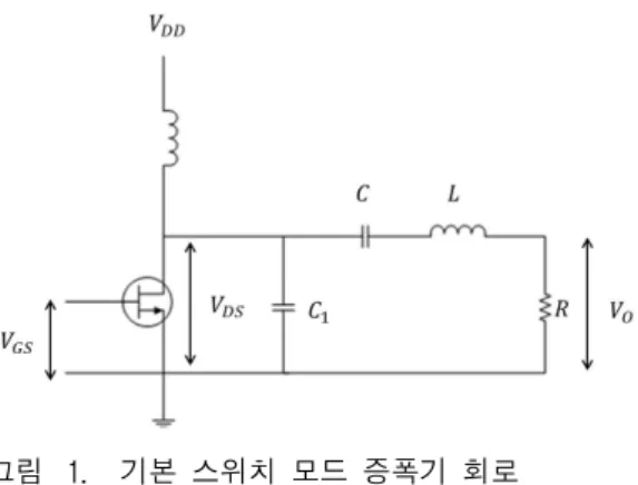
The main idea of switch-mode PA technology is to operate the transistor in saturation, so that either voltage or current, depending on amplifier class, is switched on and off. In other words the transistor is operated like the ideal switch in the switch-mode power amplifier. The voltage and current waveforms of the transistor must not overlap if the power consumption of the transistor is to be minimized, and
그림 1. 기본 스위치 모드 증폭기 회로 Fig. 1. Switch-mode amplifier basic circuit.
the high-efficiency property of the power amplifier is obtained by switching the transistor between its
“ON” and “OFF” states. Fig. 1 shows a simplified block diagram of a switch-mode power amplifier[7].
(2) Class-E power amplifier
At first proposed by Sokal, Theoretical drain efficiency of 100% can be achieved because the class-E power amplifier attains high conversion efficiency by preventing simultaneous high voltage and high current across the device. But the efficiency is affected by parasitic component, so it is not 100%
experimentally. Fig.2 shows the ideal circuit of class-E power amplifier, which consists of an ideal switch, parallel capacitor, simple resonant circuit, and specific load impedance. A class-E power amplifier is more efficient than other classes of amplifier as a result of its lower power consumption. A class-E
그림 2. Class-E 전력증폭기 (a) 구조 (b) 트렌지스터의 전압전류 파형
Fig. 2. Class-E power amplifier (a) configuration (b) voltage and current waveforms of the transistor.
power amplifier using the same operation frequency, output power, and transistor consumes 2.3 times less power than a conventional class-B or class-C power amplifier. Figure 2 (a) shows the ideal class-E power amplifier circuit, (b) shows the ideal voltage and current wave forms of transistor in the class-E power amplifier[7~[9].
Ⅲ. Theory and design of dual bias control
PAE can be expressed as Equation. (1)
× ×
(1)
In this paper, both voltages of gate and drain have been controlled by input power level. A gate and drain bias control circuit has been used by controlled both gate and drain voltages in which an envelope detector using an LTC5507 RF power detector with a good linearity and the stability.
The input signal power has been detected by a RF power detector, which controlled gate and drain
그림 3. RF 로드라인과 다양한 DC 바이어스 Fig. 3. RF load line and various DC bias point.
그림 4. 게이트와 드레인 조절 회로 Fig. 4. Gate and drain bias control circuit.
voltage for the power amplifier. The gate control voltage has been increased to level up of dc voltage of RF power detector by operation amplifier[10].
As Shown in Fig. 4 corresponding to increasing in input power, a bias control circuit has been fabricated in this research using a directional coupler due to the decrease in the gate and drain bias voltage value.
Ⅳ. Design of Power Amplifier Design
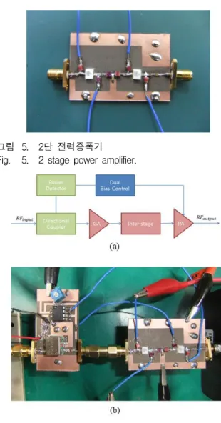
Fig. 5 shows the circuit for a two-stage class-E power amplifier consisting of a drive amplifier and a
그림 5. 2단 전력증폭기 Fig. 5. 2 stage power amplifier.
그림 6. 게이트와 드레인 바이어스 조절회로를 이용한 전력증폭기 (a) 블록도 (b) 제안된 전력증폭기 Fig. 6. Power amplifier using gate and drain bias
control circuit (a) block diagram (b) proposed power amplifier.
class-E power amplifier. The two-stage structure using the drive amplifier is adopted for the high gain property, and the class-E power amplifier structure is used for the high efficiency property. The target application of our work is in magnetic resonance. The input impedance of the antenna coil is 50Ω, therefore, the output port of the power amplifier was matched at 50 Ω.
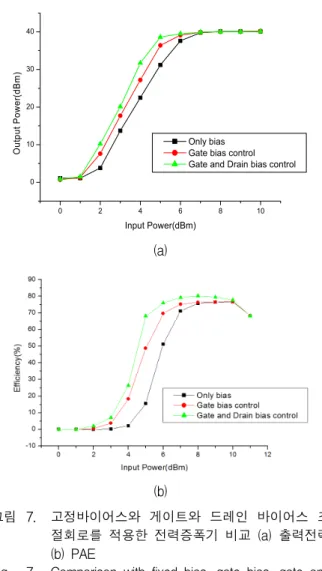
The output power of 40.17dBm was measured through an output power of 9.17dBm at 13.56MHz with the attenuator which has the measurement of the output power is -30.83dB. The drain currents of the drive amplifier and power amplifier stages are 12mA and 478mA, respectively. There for PAE is 80.5% and the gain is 30dB of the overall amplifier.
0 2 4 6 8 10
0 10 20 30 40
Output Power(dBm)
Input Power(dBm) Only bias Gate bias control Gate and Drain bias control
(a)
(b)
그림 7. 고정바이어스와 게이트와 드레인 바이어스 조 절회로를 적용한 전력증폭기 비교 (a) 출력전력 (b) PAE
Fig. 7. Comparison with fixed bias, gate bias, gate and drain bias control (a) output power (b) PAE
Fig. 6 shows block diagram of the gate and drain bias control circuit.
Ⅴ. Conclusion
In this paper, we employed the drain and gate bias control circuit to improve PAE of power amplifier.
The envelope of the input signal has been detected, and it has been used to control dc bias of the drain and gate dynamically.
As a result, we obtained the PAE about 80.5%. It has been improved 4% by the power amplifier using the gate and drain bias control circuit when compare with that of the fixed bias power amplifier.
The PAE of proposed power amplifier has been improved even at lower input power level.
REFERENCES
[1] A. Karalis, J. D. Joannopoulos, and M. Soljacic,
“Efficient wireless non-radiative mid-range energy transfer”, Annals of Physics, vol. 323, no.
1, pp.34-48, Jan. 2008.
[2] A. Kurs, A. Karalis, R. Moffatt, J. D.
Joannopoulos, P. Fisher, and M. Soljacic,
“Wireless power transfer via strongly coupled agnetic resonances, “Science, vol. 317, pp. 83-86, Jul. 2007.
[3] B. L. Cannon, J. F. Hoburg, D. D. Stancil, and S. C. Goldstein, “Magnetic resonant coupling as a potential means for wireless power transfer to multiple small receivers,” IEEE Transactions on Power Electronics, vol. 24, no. 7, pp. 1819-1825, Jul. 2009.
[4] G. Hanington, “High-efficiency power amplifier using dynamic power supply voltage for CDMA applications”, IEEE Transactions On Microwave Theory And Techniques, vol. 47, no. 8, Aug.
1999 1471-1476.
[5] Adel A. M. Saleh and D. C. Cox, “Improving the power-added efficiency of FET amplifiers operating with varying-envelope signals”, IEEE Transaction On Microwave Theory And Techniques, vol.31, no. 1, Jan 1983.
[6] T. Fowler, “Efficiency improvement techniques at low power levels for linear CDMA and
저 자 소 개 이 성 제(정회원)
2012년 2월 숭실대학교 정보통신 전자공학부 학사 졸업 2012년 2월∼현재 숭실대학교 정보통신공학과 석사과정.
<주관심분야 : 초고주파 회로설 계, RF Power Amplifier, Digital RF, 무선에너지 전송>
서 철 헌(정회원) 1983년 3월 서울대학교 전자공학과 (공학사) 1985년 3월 서울대학교 전자공학과 (공학석사) 1993년 3월 서울대학교 전자공학과 (공학박사) 1993년∼1995년 MIT 연구원
1993년∼1997년 숭실대학교 정보통신학과 조교수 1999년 8월∼2001년 1월 MIT 방문교수
1997년∼2004년 숭실대학교 정보통신 전자공학부 부교수
2005∼현재 숭실대학교 정보통신전자공학부 교수
<주관심분야 : 이동 및 위성통신 Microwave 부 품 및 시스템, PBG를 이용한 RF부품>
WCDMA power amplifiers”, Proc. of the 2002 RFIC Symp., Baltimore, pp. 41-44, June 2002.
[7] S. C. Cripps, RF Power Amplifiers for Wireless Communications, Artech House, 1999.
[8] A. Grebennikov, N. O. Sokal, Switchmode RF power Amplifiers, ewnes, 2007.
[9] N. O. Sokal and A. D. Sokal, “Class-E a new class of high efficiency tuned single-ended switching power amplifiers”, IEEE Journal of Solid-State Circuits, vol. 10, no. 3, pp. 168-176, Jun 1975.
[10] Y. S. Jeon J. K Cha, S. W. Nam,
“High-Efficiency power amplifier using novel dynamic bias switching”, IEEE Transactions on Microwave Theory And Techniques, vol. 55, no.
4, April 2007.