ETRI Journal. 2019;0(0):1–8. wileyonlinelibrary.com/journal/etrij
|
11
|
INTRODUCTION
Recently, as the number of automobiles has significantly in-creased, wireless communication technologies that provide traffic information and safety warnings to vehicles have been widely studied [1]. Until recently, the majority of studies on antennas used in the automotive industry have been fo-cused on global positioning systems (GPS), dedicated short‐ range communications (DSRCs), and tolling systems [2‒4]. However, as many communication systems such as GPS, FM/ AM radio, digital audio broadcasting, DSRC, and code divi-sion multiple access are installed in vehicles, several types of antennas are also required to be used in vehicles.
Among the types of antennas referred to above, wireless access in vehicular environment (WAVE) communication
technology, also known as the IEEE 802.11p standard, is re-quired to support intelligent transportation system applica-tions in short‐range communicaapplica-tions. WAVE systems also provide real‐time traffic information for preventing the oc-currence of accidents and reducing traffic congestion. The WAVE system operates in the frequency range of 5.850 GHz– 5.925 GHz for vehicle‐to‐vehicle (V2V) and vehicle‐to‐infra-structure communications [5].
WAVE systems mainly comprise on‐board units (OBU) installed in vehicles and roadside units used for infrastruc-ture. As the OBU antenna is installed vertically on the roof of vehicles, its height should be as small as possible while meeting performance requirements. To maintain seamless communications between fast‐moving vehicles, the beam pattern radiating from the antenna should be isotropic in the
O R I G I N A L A R T I C L E
Design and implementation of electromagnetic band‐gap
embedded antenna for vehicle‐to‐everything communications in
vehicular systems
Hongchan Kim
1|
KyuBong Yeon
2|
Wonjong Kim
3|
Chul Soon Park
1This is an Open Access article distributed under the term of Korea Open Government License (KOGL) Type 4: Source Indication + Commercial Use Prohibition + Change Prohibition (http://www.kogl.or.kr/info/licen seTyp eEn.do).
1225-6463/$ © 2019 ETRI
1School of Electrical Engineering, Korea
Advanced Institute of Science and Technology, Daejeon, Rep. of Korea
2ADAS center, Korea Automotive
Technology Institute, Cheonan, Rep. of Korea
3Seoul SW‐SoC Convergence
R&BD Center, Electronics and Telecommunications Research Institute, Daejeon, Rep. of Korea
Correspondence
Hongchan Kim, School of Electrical Engineering, Korea Advanced Institute of Science and Technology, Daejeon, Rep. of Korea.
Email: [email protected]
We proposed a novel electromagnetic band‐gap (EBG) cell‐embedded antenna struc-ture for reducing the interference that radiates at the antenna edge in wireless access in vehicular environment (WAVE) communication systems for vehicle‐to‐every-thing communications. To suppress the radiation of surface waves from the ground plane and vehicle, EBG cells were inserted between micropatch arrays. A simulation was also performed to determine the optimum EBG cell structure located above the ground plane in a conformal linear microstrip patch array antenna. The characteris-tics such as return loss, peak gain, and radiation patterns obtained using the fabri-cated EBG cell‐embedded antenna were superior to those obtained without the EBG cells. A return loss of 35.14 dB, peak gain of 10.15 dBi at 80°, and improvement of 2.037 dB max at the field of view in the radiation beam patterns were obtained using the proposed WAVE antenna.
K E Y W O R D S
automotive communication antenna, electromagnetic band‐gap, linear array antenna, micro‐strip patch, WAVE
lateral direction and have the shape of the infinity symbol (∞) when observed from a vertically cross‐sectional view. Else, the accessible distance between the vehicles or between vehicles and infrastructure will vary according to the lateral relative direction.
As the surface waves radiating from the edge of the tenna degrade the communication performance of the an-tenna (eg., in terms of efficiency and radiation pattern), it is important to reduce and control the surface waves from the antennas on vehicles. Several methods have been proposed for reducing these surface waves. One such approach involves the use of a synthesized substrate with an optimized dielec-tric constant around the patch of the antenna [6‒8]. Another approach involves building a core with a different permittiv-ity under the patch of the antenna [9]. Electromagnetic band‐ gap (EBG) introduced antenna structures can also be used to reduce surface waves [10‒12].
As some of these antennas are installed on the roof of the vehicle, the effects of interference from the roof, which mainly comprises metal, should be considered. The roof of the vehicle acts as a ground plane for the antenna. Therefore, it is necessary to conduct studies that take into consideration the effect of the vehicle's roof on WAVE communication systems.
In this paper, we report on an EBG‐based antenna struc-ture without changing the size and shape of the conformal linear microstrip patch array antenna used in WAVE commu-nication systems while considering the effects of the vehicle's roof. A simulation was performed to determine the optimum structure of the EBG cell‐embedded antenna structure. The typical characteristics of the fabricated EBG‐based antenna for WAVE systems were then analyzed.
2
|
DESIGN
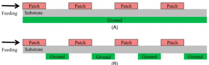
Figure 1A shows the cross‐sectional view of conventionally used vertical patch antennas, which can radiate an electric field in the forward direction. In this structure, a ground plane was formed underneath. However, to improve the typi-cal characteristics of the microstrip patch antenna, ground planes were located between the patches in improved con-ventional microstrip antennas, as shown in Figure 1B. In this
scheme, the electric field can be radiated in both the forward and backward directions, which is applicable to WAVE com-munication systems.
A single antenna [13] consists of three major parts: a se-ries of feeding lines, four antenna segments for generating the required resonant frequency, and four ground segments. However, although the ground plane was removed from the region between the patches, the radiation of the surface wave still remained, which requires to be solved.
Patches are placed on the front surface of the substrate, and the ground patterns are placed on the underneath surface between the patches. To obtain omnidirectional radiation pat-terns from the microstrip antenna for V2V communication, the ground planes were removed from under the patches. Instead of locating the ground planes just below each patch, these were located between the patches. The linear array of the rectangular structure microstrip patches is printed on a dielectric Teflon substrate with a relative dielectric constant
(εr) of 2.2 and thickness of 0.8 mm. The series of feeding lines
is connected to the coaxial cable through a 50‐Ω connector. Although the radiation patterns from the microstrip an-tenna are directional with a beam width of 80°–100°, the issue of surface wave suppression still remains. To suppress the surface waves radiating from the microstrip antenna structure, we have proposed a new type of microstrip antenna structure in which EBG cells were introduced between the patches, which is explained in detail in the next section. The EBG cell‐embedded antenna structure fabricated and charac-terized in this study is schematically presented in Figure 2. EBG cells were connected to the ground plane through metal via. Figure 2A presents a cross‐sectional view of the EBG cell‐embedded antenna structure and Figure 2B presents a magnified schematic of each EBG cell‐embedded antenna structure. To investigate the effects of the EBG cells on the suppression of surface waves, four EBG cells were located above the ground segments. The details of the structure are explained in the next section.
2.1
|
Overall structure of the antenna
The basic structure we propose comprises a series of linear array antennas composed of four antenna patches for gen-erating a frequency range of 5.850 GHz–5.925 GHz for the WAVE system, as shown in Figure 1B. The role of the center‐feed array structure is to radiate maximum power and reduce feed line losses. Furthermore, the size of the EBG cell‐embedded antenna can be as small as possible in a direc-tion transverse to the array axis, as shown in Figure 1B.
A use of a series of feed linear array antennas in a con-ventional structure has some drawbacks, including the gener-ation of surface waves [14]. Surface wave genergener-ation reduces the efficiency of the antenna and degrades the radiation beam patterns emitted from the antenna. In this study, in order to
FIGURE 1 Schematics of a (A) conventional and (B) improved conventional microstrip antenna for WAVE communication system
Patch Ground Patch Patch Ground Patch Ground Ground Feeding Substrate Patch Ground
Patch Patch Patch
Feeding Substrate
(A)
reduce these effects of array antennas on a thick and high‐ permittivity substrate, four antenna patches were separated by EBG cells over the ground plane.
2.2
|
EBG cell structure
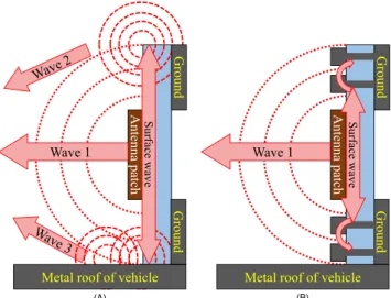
We investigated the generation of surface waves in a con-ventional vertically placed patch antenna structure before de-signing the EBG cell‐embedded antenna structure. Figure 3A shows the appearance of the space and surface waves that ra-diate from the conventional antenna without the use of EBG cells. In addition to the space waves (denoted as wave 1), the surface waves were generated in the high–dielectric constant layer between the patch and ground plane and which then radiate from the floating edges (denoted as wave 2), or are reflected away onto the roof of the vehicle (denoted as wave 3). In the conventional antenna system, a phase shift occurs
owing to the metal ground plate, thus resulting in construc-tive interference. Figure 3A shows the phase shift caused by the finite ground plane formed by the metal. The surface wave appearing at the edge of the ground plane contributes to the radiation pattern in the conventional antenna structure.
The space waves radiating from the patches, surface waves radiating from the floating edge, and the waves reflected at the roof of the vehicle were combined, thus resulting in the formation of a series of multipath lobes and nulls at various angles. The multipath interference of waves 1, 2, and 3 dis-torts the radiation pattern. Therefore, to reduce multipath in-terference, the generation of surface waves from the patch antenna should be suppressed.
In this work, we propose an EBG‐inserted patch antenna to suppress the generation of surface waves, as shown in Figure 3B. By blocking the surface waves with EBG cells placed be-tween the antenna patches, the surface waves are prevented from propagating on the ground patches and metal roof of the vehicle. Therefore, any induced currents are restricted to a lo-calized region around the antenna patches and cannot reach the edges of the ground patches. Thus, surface waves can be suppressed in the EBG cell‐embedded antenna structure.
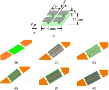
Using the above‐mentioned design concept, we designed a mushroom‐like EBG cell structure, as shown in Figure 4A. In this design, we have considered various widths (w) of square‐ shaped EBG cells and gaps (g) between the EBG cells, as presented in Figure 4B–4G. Mushroom‐like EBG cells are periodically inserted between the antenna patches. Each cell is composed of a square‐shape metal head connected to a ground patch through a dielectric‐substrate via.
The resonance frequency of the antenna can be calculated using the following equations reported in [12]:
where L is the inductance, C is the capacitance, W is the width of a patch, g is the gap between the EBG cells, h is the height of the EBG cell, μ0 is the permittivity in free space, ε0
is the dielectric constant in free space, and εr is the relative
dielectric constant of the substrate. The bandwidth of the EBG is given by.
where 𝜂=√𝜇0∕𝜀0 is the impedance in free space.
The impedance of a parallel resonant LC circuit is given by. (1) 𝜔o= 1 √ LC , (2) L= 𝜇0h, (3) C= W𝜀0(1 + 𝜀r ) 𝜋cosh−1[W+g g ], (4) Bandwidth= 1 𝜂 √ L∕C ,
FIGURE 2 Schematics of cross‐sectional view of (A) proposed EBG cell‐embedded antenna and (B) magnified view of unit EBG‐ embedded antenna structure
Patch Ground Patch Patch Ground Patch Ground Ground Feeding Substrate
EBG cell structures
Height of EBG cell Microstrippatch
Width of EBG cell
Gap between EBG cells Ground plane Substrate 9 nm (A) (B)
FIGURE 3 Space and surface waves radiated from (A) conventional and (B) proposed EBG cell‐embedded antenna structure
Antenna patc
h
Ground
Ground
Metal roof of vehicle
Wave 1 Surface wave Antenna patc h Wave 1 Ground
Metal roof of vehicle
Surface wave
Ground
The impedance is very high at the resonance frequency of
ω0. The capacitors are formed by the fringing electric fields
between the adjacent metal mushroom head, and the induc-tance is fixed according to the thickness of the structure.
3
|
RESULTS AND DISCUSSION
To obtain an optimized EBG cell‐embedded antenna struc-ture, we performed a simulation using the high‐frequency structure simulator (HFSS) program for various widths (w) of square‐shaped EBG cells and gaps (g) between the
EBG cells while keeping the size of the ground plane as 9 mm × 15 mm, as depicted in Figure 4A. In this simula-tion, the height of the EBG cells (h) was fixed as 0.835 mm. The thickness of the substrate and metal mushroom head formed on top of the substrate were 0.8 mm and 0.035 mm, respectively. The simulation was performed by assuming an ideal environment in which no manufacturing toler-ance or measurement environment effects were taken into consideration.
The antenna for WAVE communication used in the simulation and measurement was installed on roof of the vehicle (see Figure 5). The overall size of the proposed
antenna is 9 × 137.5 mm2, and the size of each patch
antenna is 9 × 15 mm2, as shown in Figure 5A. These
sizes were selected to satisfy the resonance frequency and bandwidth for WAVE communication. Based on the simu-lation results, we fabricated three types of EBG cells with different dimensions by varying w and g, as illustrated in Figures 4D, 4E, and 4F.
The fabricated antenna was analyzed in an electromag-netic anechoic chamber in a middle‐level vacuum environ-ment to minimize other environenviron-mental effects and evaluate the effects of EBG cells on surface wave suppression, as pre-sented in Figure 6.
Figure 6A presents photo images of the measurement setup of the fabricated EBG cell‐embedded antenna and Figure 6B shows magnified images of the EBG cell‐embed-ded antenna used in these measurements. In the measurement environment, the manufacturing tolerance should be taken into consideration and compared to the results obtained in the simulation, which is explained later.
Figure 7 shows the simulation and measurement results
of the reflection coefficient (S11) for various values of w and
g, which implies that the number of EBG cells is also varied.
As w and g decrease, S11 decreases significantly, as shown
in Figure 7. S11 decreases owing to the low‐impedance
sur-face. Moreover, as the number of EBG cells increase, S11 also
decreases, as in the case of the decreased values of w and (5)
Z= j𝜔L
(1 − 𝜔2LC).
FIGURE 4 (A) Schematic of EBG cells with dimensions. Each EBG cell is connected to the ground plate via a metal electrode. Schematics of antenna structures (B) without EBG cell, (C) 4 × 7 (w = 2 mm, g = 0.2 mm), (D) 6 × 10 (w = 1 mm, g = 0.5 mm), (E) 8 × 15 (w = 1 mm, g = 0.1 mm), (F) 14 × 26 (w = 0.5 mm, g = 0.1 mm), (G) 14 × 28 (w = 0.5 mm, g = 0.05 mm) x y 9 mm 15 mm w g h (A) (B) (C) (D) (E) (F) (G)
FIGURE 5 (A) Schematic of the proposed EBG cell‐embedded antenna used in the measurement; (B) Photo image of one of the fabricated proposed antennas (8 × 15 (w = 1 mm, g = 0.1 mm)) Top layer Bottom layer x y z Substrate
Feed line Antenna
35 mm 137.5 mm
9 mm
SMA
(A)
g. However, as w and g were further decreased, especially
below 0.5 mm and 0.1 mm, respectively, S11 increased. The
increase in S, when the w and g values were less than 0.5 mm
and 0.1 mm, respectively, can be attributed to the low imped-ance, which can be calculated using (3) and (5). Thus, when the values of w and g are too small, the impedance in the EBG cell‐embedded antenna may not be sufficiently high, thus re-sulting in an increased return loss.
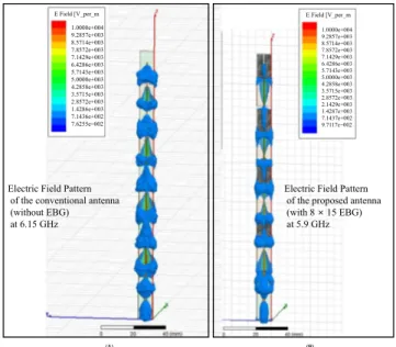
Figures 8A and 8B show the simulation results of the ra-diated electric field patterns obtained from conventional and EBG‐embedded microstrip antennas, respectively. The fre-quencies used in Figure 8 to obtain of these patterned plots are 6.15 GHz (without EBG cell) and 5.9 GHz (with 8 × 15
EBG cells), respectively, which shows the lowest S11 value
obtained in Figure 7.
As shown in Figure 8A, a relatively weak electric field was observed between the patches. In contrast, the electric field was almost suppressed in the EBG cell‐embedded mi-crostrip antenna as presented in Figure 8B. The electric field from the patches propagated toward the direction of the EBG cells. As the EBG cells were connected to the ground plate via a metal electrode, the electric field intensity can be re-duced in the region of the EBG cells. It might be considered that by reducing electric field intensity in the EBG cell–in-serted area, the surface waves can be also suppressed in the same region, which is the key role of the EBG cells.
Although we fabricated three types of EBG cell‐ embedded antennas with different values of w and g, the 8 × 15 EBG cell‐embedded antenna, for which w = 1 mm,
g = 0.1 mm, exhibited the best characteristics among the
fabricated EBG cell‐embedded antennas. Therefore, we an-alyzed the 8 × 15 EBG cell‐embedded antenna in greater detail. In Table 1, we present a comparison of the simulation
and measurement values of S11, peak gain, and radiation
efficiency for the various EBG structures. The simulation
FIGURE 6 (A) Measurement environment and (B) magnified photo image of measurement setup of fabricated EBG cell‐embedded antenna
Signal detector
(A)
(B)
FIGURE 7 Simulation and measurement results of reflection coefficient of the proposed antenna as a function of frequency with different sizes of w and g. The measurement was performed using the structure shown in Figure 4E
–50 –45 –40 –35 –30 –25 –20 –15 –10 –5 0 5.0 5.6 6.1 6.7 S11 (dB) Frequency (GHz)
Without EBG simulation With EBG simulation (width: 1 mm, gap: 0.5 mm) With EBG simulation (width: 1 mm, gap: 0.1 mm) With EBG simulation (width: 0.5 mm, gap: 0.05 mm) With EBG Measurement (width: 1 mm, gap: 0.1 mm)
FIGURE 8 Simulation results of the radiated electric field pattern of the (A) conventional antenna (without EBG cell) and (B) EBG cells‐embedded antenna structure
Electric Field Pattern of the conventional antenna (without EBG) at 6.15 GHz
Electric Field Pattern of the proposed antenna (with 8 15 EBG) at 5.9 GHz E Field [V_per_m 1.0000e+004 9.2857e+003 8.5714e+003 7.8572e+003 7.1429e+003 6.4286e+003 5.7143e+003 5.0000e+003 4.2858e+003 3.5715e+003 2.8572e+003 1.4286e+003 7.1436e+002 7.6255e 002 E Field [V_per_m 1.0000e+004 9.2857e+003 8.5714e+003 7.8572e+003 7.1429e+003 6.4286e+003 5.7143e+003 5.0000e+003 4.2858e+003 3.5715e+003 2.8572e+003 2.1429e+003 1.4287e+003 7.1437e+002 9.7117e 002 (A) (B)
results show that the proposed EBG cell‐embedded antenna model improves the peak gain from 8.6 dBi (without EBG cell) to 11.24 dBi (with 8 × 15 EBG cells). The 8 × 15 EBG cells have the values of w and g as 1 and 0.1 mm, respec-tively. Moreover, the measured peak gain also improves from 8.113 dBi at 90° (without EBG cell) to 10.15 dBi at 80° (with 8 × 15 EBG cells). The measured S11 improves from −14.58 dB (without EBG cell) to −35.14 dB (with 8 × 15 EBG cells), as shown in Table 1.
The discrepancy of the peak gain between the simulation and measurement results can be attributed to factors such as manufacturing tolerance and measurement environment. As mentioned previously, the simulation performed using the
HFSS program was for the ideal case, which means the pre-cise values of w and g. In contrast, the values of w and g can be slightly different for those used in the measurement owing to the manufacturing tolerance during the fabrication step. Moreover, the electromagnetic anechoic chamber gain dis-crepancy in the measurement environment could also cause a discrepancy.
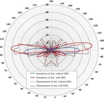
The radiation beam patterns of the antenna located ver-tically on the roof of the vehicle are shown in Figure 9. The measurement results were measured at 10° increments, and the simulations were performed at 2° increments. The pro-posed EBG cell‐embedded antenna showed a 2.037 dB gain over the field of view as compared with the conventional antenna model without EBG cells. The radiation beam pat-terns have the shape of an infinity symbol in the vertical cross‐sectional view, which enables seamless communi-cations between fast moving vehicles and an accessible distance for vehicle communications. In WAVE communi-cation systems, a minimum return loss of 9.5 dB and volt-age swing ratio of 2.0 over the field of view are required. As per the above simulation and measurement results, the EBG cell‐embedded antenna structure satisfies the basic requirements of WAVE communication systems, which means that the results of our study can be applied to WAVE communication systems.
Figure 10 shows the simulation and measurement results of the gain obtained from the 8 × 15 EBG cell‐embedded antenna structure. For use in WAVE communication system, beam patterns from antenna should be radiated in both direc-tions. However, in conventional antenna structures, as sche-matically illustrated in Figure 1A, beam patterns were radiated in the upward direction, and there were no beam patterns in the ground plane. Therefore, the ground planes were moved between the patches to radiate beam patterns in both direc-tions. Although the radiated beam patterns appeared in both directions in conventional microstrip antenna structures as
TABLE 1 Comparison of S11, peak gain, and efficiency obtained in simulation and measurement with and without EBG cells
S11 [dB] Peak Gain [dBi]
Radiation efficiency (%)
Simulation Measurement Simulation Measurement
No EBG cells –24.50 –14.58 8.60 8.113 98.6 4 × 7 EBG cells (w/g = 2/0.2 mm) –17.13 N/A 9.98 N/A 98.5 6 × 10 EBG cells (w/g = 1/0.5 mm) –28.96 –20.31 10.49 9.890 98.1 8 × 15 EBG cells (w/g = 1/0.1 mm) –33.17 –35.14 11.24 10.150 98.6 14 × 26 EBG cells (w/g = 0.5/0.1 mm) –27.00 N/A 10.46 N/A 98.4 14 × 28 EBG cells (w/g = 0.5/0.05 mm) –24.58 –18.27 10.35 9.590 97.9
FIGURE 9 Simulation and measurement results of radiation beam patterns obtained from antennas without EBG and with EBG cells
Simulation of Ant. without EBG Simulation of Ant. with EBG Measurement of Ant. without EBG Measurement of Ant. with EBG
shown in Figure 1B, the surface wave radiation still remains. To suppress the surface wave, EBG cells were embedded be-tween the patches and connected to the ground via a metal electrode. In EBG cell‐embedded antenna structures, the beam patterns can be radiated in both directions and the beam peak can be observed at both the front and back, as shown in Figure 10 with a suppressed surface wave. Therefore, it is sug-gested that EBG cell‐embedded microstrip antenna structures are suitable for WAVE communication systems as the beam patterns can be radiated in both the forward and backward directions with a suppressed surface wave.
We can conclude that the optimum number of EBG cells to suppress surface waves in WAVE communication systems is 8 × 15. As the number of EBG cells is 8 × 15, we can ob-tain a highly improved return loss, improved radiation beam pattern values, and an improved peak gain.
4
|
CONCLUSION
The proposed EBG cell‐embedded antenna system effi-ciently suppressed surface waves with a decreased return loss of 35.14 dB and an increased peak gain of 10.15 dBi at 80°. The measurement results confirmed that the pro-posed EBG cell‐embedded antenna structure can improve
the performance of the antenna in WAVE communication systems. Furthermore, the gain over the field of view in-creased by up to 25% as compared with the conventional antenna model without the EBG structure. The optimum number of EBG cells is 8 × 15, while considering the re-flection coefficient, radiation beam pattern, and peak gain. The improved performance of the EBG cell‐embedded antenna can increase the connectivity of vehicle‐to‐every-thing communications in WAVE systems.
ORCID
Hongchan Kim https://orcid.org/0000-0002-4246-1839
REFERENCES
1. P. Papadimitrator et al., Vehicular communication systems:
en-abling technologies, applications, and future outlook on intelligent transportation, IEEE Commun. Mag. 47 (2009), no. 11, 84–95.
2. T. Varum et al., Printed antenna for DSRC systems with
omnidirec-tional circular polarization, in Int. IEEE Conf. Intell. Transport.
Syst., Anchorage, AK, USA. September, (2012), 475–478. 3. S. Arianos et al., Design of multi‐frequency compact antennas
for automotive communications, IEEE Trans. Antenn. Propag. 60
(2012), no. 12, 5604–5612.
4. A. Ghobadi and M. Dehmollaian, A printed circularly polarized
Y‐shaped monopole antenna, IEEE Antenn. Wireless Propag. Lett. 11 (2012), no. 11, 22–25.
5. R.A. Uzcategui, A.J. De Sucre, and G. Acosta‐Marum, WAVE: a
tutorial, IEEE Commun. Mag. 47 (2009), no. 5, 126–133.
6. G.P. Gauthier, A. Courtay, and G.M. Rebeiz, Microstrip
anten-nas on synthesized low dielectric‐constant substrate, IEEE Trans.
Antenn. Propag. 45 (1997), 1310–1314.
7. I. Papapolymerou, R.F. Drayton, and L.B. Katehi, Micromachined
patch antennas, IEEE Trans. Antenn. Propag. 46 (1998), no. 2,
275–283.
8. J.S. Colburn and Y. Rahmat‐Samii, Patch antennas on
exter-nally perforated high dielectric constant substrates, IEEE Trans.
Antenn. Propag. 47 (1999), no. 12, 1785–1794.
9. D.R. Jackson et al., Microstrip patch antenna designs that do not
excite surface waves, IEEE Trans. Antenn. Propag. 41 (1993), no.
8, 1026–1037.
10. D. Sievenpiper et al., High‐impedance electromagnetic surfaces
with a forbidden frequency band, IEEE Trans. Micro. Th. Tech. 47
(1999), no. 11, 2059–2074.
11. F. Yang and Y. Rahmat‐Samii, Microstrip antennas integrated with
electromagnetic band‐gap (EBG) structures: a low mutual cou-pling design for array application, IEEE Trans. Antenn. Propag. 51 (2003), no. 10, 2936–2946.
12. A. Verma et al., EBG structure and its recent advances in
micro-wave antenna, J. Sci. Res. Eng. Technol. 1 (2012), 84–90.
13. H. Kim et al., A high performance EBG antenna design for WAVE
communication systems, in IEEE Int. Symp. Consum. Electron.,
Jeju Island, Rep. of Korea, August, (2014). pp. 1–4.
14. A. Benalla et al., Design of a low side lobe short series‐fed linear array of microstrip patches, Electromag. Lab. Sci. Report 93, Dept. of ECE, Univ. ofColorado, Boulder, Oct. 1987.
FIGURE 10 (A) Simulation and (B) measurement results of radiation peak gain obtained from the proposed EBG cell‐embedded antenna dB (GainTotal)*1 1.1244e+001 6.5200e+000 1.7958e+000 –2.9284e+000 –7.6526e+000 –1.2377e+001 –1.7101e+001 –2.1825e+001 –2.6549e+001 –3.1273e+001 –3.5998e+001 –4.0722e+001 –4.5446e+001 –5.0170e+001 –5.4894e+001 –5.9618e+001 –6.4343e+001 z Theta y Phi Peak value: 10.150 Peak point: 80, 80 z – 17.999 Peak 1.150 0.767 –8.616 – 27.382 Min y x y z x y z (A) (B)
AUTHOR BIOGRAPHIES
Hongchan Kim received his MS
de-gree in Electronics Engineering from the Korea Advanced Institute of Science and Technology (KAIST), Daejeon, Rep. of Korea, in 2005. He is currently pursuing the PhD degree in Electronics Engineering from KAIST. From 2005 to 2015, he worked for the Korea Evaluation Institute of Industrial Technology, Daejeon, Rep. of Korea. Since 2015, he has been with the Korea Technology and Information Promotion Agency for SMEs, Daejeon, Rep. of Korea, where he is now a head of office. His main re-search interests are automotive semiconductor design and robust RF system design.
KyuBong Yeon received his MS and
PhD degrees in Electronics Engineering from Hanyang University, Seoul, Rep. of Korea, in 2000 and 2014, respec-tively. Since 1995, he has been with the ADAS center, Korea Automotive Technology Institute, Cheonan, Rep. of Korea, where he is now a director. His main research interests are automotive semiconductor design and robust RF system design.
Wonjong Kim received his MS and
PhD degrees in Electronics Engineering from Hanyang University, Seoul, Rep. of Korea, in 1992 and 1999, respectively. Since 2000, he has been with Electronics and Telecommunications Research Institute, Daejeon, Rep. of Korea, where he is now a principal researcher. His main research interests are SoC design methodology, virtual SoC platforms, and ma-chine learning hardware acceleration.
Chul Soon Park received the BS
de-gree from Seoul National University, Seoul, Rep. of Korea in 1980, and the MS and PhD degrees in materials sci-ence and engineering from the Korea Advanced Institute of Science and Technology (KAIST), Daejeon, Rep. of Korea, in 1982 and 1985, respectively. From 1985 to 1999, he worked with the Electronics and Telecommunication Research Institute, Daejeon, Rep. of Korea, where he contributed to the development of semi-conductor devices and circuits. From 1987 to 1989, he studied the very initial growth of group IV semiconduc-tors during a visit to AT&T Bell Laboratories, Murray Hill, NJ, USA. Since 1999, he has been with the Information and Communications University (which merged with KAIST in 2009), where he is a full professor with the Engineering School and director of the Intelligent Radio Engineering Center. His research interests include reconfigurable RF integrated circuits, millimeter‐wave in-tegrated circuits, and their system‐on‐chip / system‐on‐ package integration.