θ
θ
θ
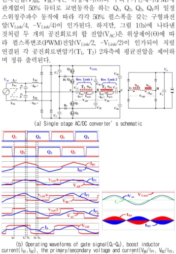
(a) Single stage AC/DC converter’s schematic
(b) Operating waveforms of gate signal(Q1~Q4), boost inductor
current(IB1,IB2), the primary/secondary voltage and current(VAB/IP1, VBC/IP2,
VAC/IP1, VAC/IS) and AC input voltage/current(Va,Ia)
Fig. 1. Single stage AC/DC converter and its operating waveforms
ϯ
ϯ
290
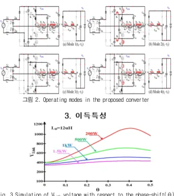
그림 2. Operating modes in the proposed converter
Fig. 3 Simulation of VLink voltage with respect to the phase-shift( )θ
θ θ θ θ cos
θ θ그림 4. Voltage gain characteristics of the proposed converter
θ
Table 1 Main input/output specifications and parameters
(a) 100VDC(200W)fs=276kHz (b) 400VDC(1kW) fs=230kHz
Fig. 5. Simulation waveforms of gate signals(Q1~Q4), boost inductor
current(IB1,IB2), the resonant tank(VAB/IP1,VBC/IP2, VAC/IP1, VAC/IS)
Hiroto Mizutani, Tomokazu Mishima, Mutxuo Nakaoka, “A Dual Pulse Modulated Five-Element Multi-Resonant DC-DC Converter and Its Performance Evaluations”, 2013 IEEE Energy Conversion Congress and Exposition, pp.4912-4919, Sept. 2013
ES Kim, T Marius, MJ Kim, JS Oh, GW Lee, IG Hwang, “A Single-Phase Single-Stage Three-Level AC/DC Resonant Converter Operating with a Wide Output Voltage Range”, 2019 IEEE APEC, March. 2019