A Simulator Design and Abnormal Signals Evaluation for the Circuit Analysis System
Kil Mo Koo, Sang Baik Kim, Hee Dong Kim, Hee Yong Kang
Korea Atomic Energy Research Institute, DukJin Dong, YuSeong, DaeJeon, 305-353, Korea [email protected]
1. Introduction
The circuit simulation analysis and diagnosis methods are used to assess instruments in detail when they give apparently abnormal readings[1-4]. In this paper, new simulator through an analysis of the important circuits modeling under severe accident conditions has been designed, the designed simulator which was composed of LabVIEW code as a main tool and then out-put file of the PSpice code as an engine tool exported to in-put file of the LabVIEW code. A procedure of a simulator design was divided by two design step, of which the first step is the diagnosis methods, the second step is the circuit simulator for the signal processing tool. It has three main functions which are a signal processing tool, an accident management tool, and an additional guide from the initial screen. This simulator should be set up in a laboratory and the signals evaluated under various degraded conditions.
2. Design Step of the Circuit Simulation and
Diagnosis Methods
2.1 Design Step of the Diagnosis Methods
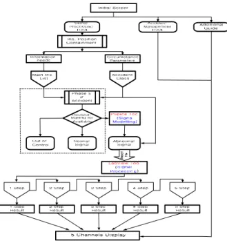
When an instrument which is providing information for managing a severe accident is apparently malfunctioning, a series of steps can be taken which include a direct diagnosis of the instrument and an indirect method of determining the value of the parameter. These methods are identified by eleven step processes and five of the steps are called operational aids. They are combinations of diagnostic actions and other means of measurement. These can be applied when instrument readouts are suspectful or faulty. The five types of aids are the diverse indication, parameter inference, portable instrument, circuit diagnosis, and the portable circuit readout. Figure 1 is flow chart of the design step for the circuit diagnosis methods.
Fig. 1 Flow chart of the design step for the circuit diagnosis
methods
2.2 Design Step of the Circuit Simulator
Figure 2 shows a flow chart of the design step for the simulator. It has three main functions which are a signal processing tool, an accident management tool, and an additional guide from the initial screen. The signal processing tools have main position information obtained from 5 areas in the containment building which include information needs of the instruments, and circumstance parameters from the accidents class. As the next step, we need the decision making from some signals which mean three kinds of signal patterns, of which first one is normal condition signals, second one is abnormal signals, and third one is out of control signals. In case of abnormal signals, they have been processed to the five step and finally they can be shown on CRT screen with enhanced signals. There are two codes to be used, the designed simulator which was composed of LabVIEW code as a main tool and the PSpice code file as an engine tool which should be exported to the LabVIEW code file.
Fig. 2 Flow chart of the design step for the simulator 3. Design Requirements and Functions
3.1 PSpice Requirement and functions
The Pspice circuit analysis program was used to study the effects of the instrument loop hardware degradation on the measurement. This information is useful for obtaining a correlation between the observations in the control room and Transactions of the Korean Nuclear Society Autumn Meeting
the actual circuit conditions. Although the goal was to develop a simple model, the intricacies of developing the appropriate waveforms and incorporating the effects of the induced noise into the circuit turned a degraded circuit loop into lines and lines of netlists, as a 4~20mA loop were used to measure the reactor coolant pressure. Figure 3 represents the circuit model as modified to run in Pspice.
V1 24V R3 10Mohm C4 100uF C1 0.2nF Rout 50ohm C2 4.4nF R4 0.4ohm L1 14.5uH R5 0.4ohm L2 14.5uH R6 0.4ohm L3 14uH Land 10uH C3 0.02nF R7 10Mohm C5 0.01nF R8 10Mohm R9 10Mohm R10 0.1ohm C6 33nF R11 10Mohm R12 10Mohm R1 1ohm C7 2.2nF R2 10Mohm R13 10Mohm C8 4.4nF Rand 0.01ohm C9 4.4nF C10 0.01nF C11 0.02nF R14 10Mohm D1 DIODE_VIRTUAL R15 1kohm Detector 0A 16mA 1Hz A B T G XSC1
Control Room 1000ft Cable-16CA.
Twisted Pair Shielded Transmitter
Fig.3 Circuit model as modified to run in PSpice.
3.2 LabVIEW Requirement and functions
There are many built-in steps available for immediate use in the code. Measurement can be quickly performed on a signal by selecting a step from the following step.
- Signal input/output-generation and acquisition of signals from a variety of hardware or software - Time domain-amplitude and level measurements,
timing and transition, and histogram
- Frequency domain-measurement for power, frequency response, tone, and distortion
- User-defined step-call any LabVIEW-VI measurement or analysis function
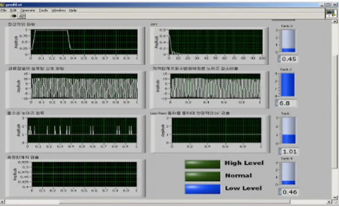
- The additional functions of the signal analysis also have oscilloscope function, FFT, IFFT, filtering, averaging, and scaling and so on.
4. 4~20mA Loop Circuit Modeling, Simulation, and
Evaluation
The loop circuit was composed of three functions which included the pressure transmitter section, the twisted shielded pair connection cable section, and the receiver section. The pressure transmitter has been simplified to obtain an equivalent representation of the resisters, capacitors, and inductors. It also includes voltage or current sources that can be varied through the circuit analysis program to obtain realistic circuit responses from environmental changes in the containment. The specific parameter includes: Input leakage (shunt) resistance that is affected by damages to the interconnecting cable. Input series resistance to represent the spliced connections that might be affected by corrosion. Input capacitance is easily increased by water intrusion into the cable or the transmitter housing. Capacitance for the ground is easily increased by the presence of water. A diode and load resistors represent the power supply current. A current generator represents the actual transmitter output signal. The typical cable is represented to describe the wire inductance
and resistance and the dielectric capacitance. The shield is represented as a third conductor. It is simplified to eliminate all the resistance and to model only the inductance and capacitance. The voltage source drives a current to a voltage sensing resistor in series with the transmitter. The negative sides of the voltage source and the shields are attempted for the ground in this analysis. Figure 4 shows input and output signals from the simulator with 4 channels.
Fig. 4 4 channels each signal from circuit simulator
5. Summary and Conclusions
In this paper, we provided a design step of the circuit simulation and diagnosis methods and showed how a circuit evaluation fits into the process as design requirements and functions.
To check malfunctions or abnormal indications from the instruments, three loops of the circuit modeling were simulated by the PSpice code, and then the PSpice code file was used as an engine tool which should be exported to the LabVIEW code file. In case of abnormal signals, they have been processed to the five steps and finally they can be show on CRT screen with enhanced signals. Using the results, a simulator can be also developed by the diagnosis logic in the severe conditions
ACKNOWLEDGEMENT
This study has been carried out under the nuclear R&D program by the Korean Ministry of Science and Technology
.
REFERENCES
[1] C. A. Negin, et al., “Instrument Performance under Severe Accident Conditions" TR-102371, Final Report, 1993.
[2] K. M. Koo, et, al., "Assessment of Existing Ul-Jin 3~4 Plants Instrumentation for Severe Accident Management" KSNP Fall Conference, 2004.
[3] M. E. Yancey, and R, C. Strahm, "Examination and Evaluation of THI-2 Transmitters CF-1-PT4 and CF-2-LT$", GEND-INF-029 Vol. III, 1985.
[4] A. J. Horn, R. W. James, D. E. True, "Assement of Existing Plant Instrumentation for Severe Accident Management" EPRI